Rev. 5.00, 09/03, page 744 of 760
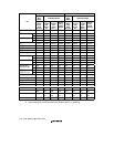
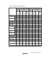
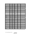
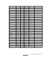
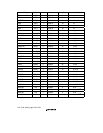
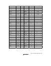
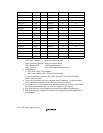
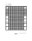
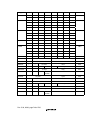
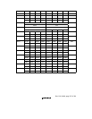
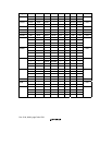
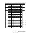
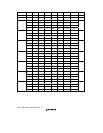
Control Register Module
*
1
Bus
*
2
Address
*
4
Size (Bits) Access Size (Bits)
*
3
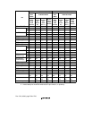
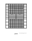
SCSMR1 IrDA P 4000140 8 8
SCBRR1 IrDA P 4000142 8 8
SCSCR1 IrDA P 4000144 8 8
SCFTDR1 IrDA P 4000146 8 8
SCSSR1 IrDA P 4000148 16 16
SCFRDR1 IrDA P 400014A 8 8
SCFCR1 IrDA P 400014C 8 8
SCFDR1 IrDA P 400014E 16 16
SCSMR2 SCIF P 4000150 8 8
SCBRR2 SCIF P 4000152 8 8
SCSCR2 SCIF P 4000154 8 8
SCFTDR2 SCIF P 4000156 8 8
SCSSR2 SCIF P 4000158 16 16
SCFRDR2 SCIF P 400015A 8 8
SCFCR2 SCIF P 400015C 8 8
SCFDR2 SCIF P 400015E 16 16
SDIR UDI I 4000200 16 16
Notes: 1. Modules:
CCN: Cache controller UBC: User break controller
CPG: Clock pulse generator BSC: Bus state controller
RTC: Realtime clock INTC: Interrupt controller
TMU: Timer unit SCI: Serial communication interface
2. Internal buses:
L: CPU, CCN, cache, TLB connected
I: BSC, cache, DMAC, INTC, CPG, and UDI connected
P: BSC and peripheral modules (RTC, TMU, SCI, SCIF, IrDA, A/D, D/A, DMAC,
PORT, CMT) connected
3. The access size shown is for control register access (read/write). An incorrect result
will be obtained if a different size from that shown is used for access.
4. To exclude area 1 control registers from address translation by the MMU, set the first 3
bits of the logical address to 101, to locate the registers in the P2 space.
5. With 16-bit access, it is not possible to read data in two registers simultaneously.
6. With 32-bit access, it is possible to read data in the register at [accessed address + 2]
simultaneously.


