Rev. 5.00, 09/03, page 284 of 760
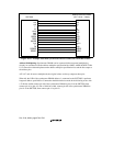
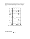
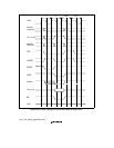
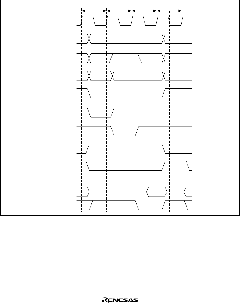
Single Read: Figure 10.16 shows the timing when a single address read is performed. As the burst
length is set to 1 in synchronous DRAM burst read/single write mode, only the required data is
output. Consequently, no unnecessary bus cycles are generated even when a cache-through area is
accessed.
CKIO
A
25 to A16,
A
13
A
12
A
15, A14,
A
11 to A0
CS2 or CS3
RAS3x
CASx
RD/WR
DQMxx
D31 to D0
BS
Tr Tc1 Td1 Tpc
Figure 10.16 Basic Timing for Synchronous DRAM Single Read


