Rev. 5.00, 09/03, page 247 of 760
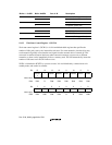
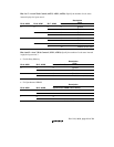
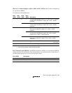
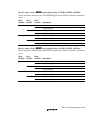
Bits 6 to 3—Address Multiplex (AMX3, AMX2, AMX1, AMX0): Specify address multiplexing
for synchronous DRAM.
For Synchronous DRAM Interface:
Bit6:
AMX3
Bit5:
AMX2
Bit 4:
AMX1
Bit 3:
AMX0 Description
1101The row address begins with A10 (The A10 value is output at
A1 when the row address is output. 4M × 16-bit × 4-bank
products)
1 0 The row address begins with A11 (The A11 value is output at
A1 when the row address is output. 8M × 16-bit × 4-bank
products)
*
1
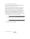
0100The row address begins with A9 (The A9 value is output at A1
when the row address is output. 1M × 16-bit × 4-bank
products)
1 The row address begins with A10 (The A10 value is output at
A1 when the row address is output. 2M × 8-bit × 4-bank
products, 2M × 16-bit × 4-bank products)
1 1 The row address begins with A9 (The A9 value is output at A1
when the row address is output. 512k × 32-bit × 4-bank
products)
*
2
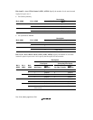
0000Begin synchronous DRAM access after setting AMX3 to 0 =
*1** (Initial value)
Except above value Reserved (Setting prohibited)
Notes: 1. Can only be set when using a 16-bit bus width.
2. Can only be set when using a 32-bit bus width.
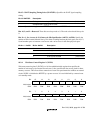
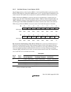
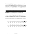
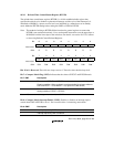
Bit 2—Refresh Control (RFSH): The RFSH bit determines whether or not synchronous DRAM
refresh operations are is performed. If the refresh function is not used, the timer for generation of
periodic refresh requests can also be used as an interval timer.
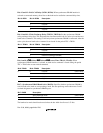
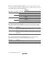
Bit 2: RFSH Description
0 No refresh (Initial value)
1Refresh


