Rev. 5.00, 09/03, page 522 of 760
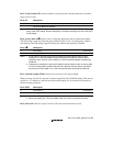
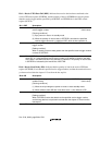
Bits 1 and 0—Clock Enable 1 and 0 (CKE1, CKE0): Select the SCIF clock source and enable
or disable clock output from the SCK pin. Depending on the combination of CKE1 and CKE0, the
SCK pin can be used for serial clock output or serial clock input.
The CKE0 setting is valid only when the SCIF is operating on the internal clock (CKE1 = 0). The
CKE0 setting is ignored when an external clock source is selected (CKE1 = 1). Before selecting
the SCIF operating mode in the serial mode register (SCSMR), set CKE1 and CKE0. For further
details on selection of the SCIF clock source, see table 16.7 in section 16.3, Operation.
Bit 1: CKE1 Bit 0: CKE0 Description
0 0 Internal clock, SCK pin used for input pin (input signal is
ignored) (Initial value)
1 Internal clock, SCK pin used for clock output
*
1
1 0 External clock, SCK pin used for clock input
*
2
1 External clock, SCK pin used for clock input
*
2
Notes: 1. The output clock frequency is 16 times the bit rate.
2. The input clock frequency is 16 times the bit rate.
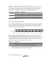
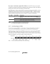
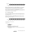
16.2.7 Serial Status Register (SCSSR)
The serial status register (SCSSR) is a 16-bit register. The upper 8 bits indicate the number of
receive errors in the SCFRDR data, and the lower 8 bits indicate the SCIF operating state.
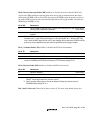
The CPU can always read and write to SCSSR, but cannot write 1 to the status flags (ER, TEND,
TDFE, BRK, OPER, and DR). These flags can be cleared to 0 only if they have first been read
(after being set to 1). Bits 3 (FER) and 2 (PER) are read-only bits that cannot be written. SCSSR is
initialized to H'0060 by a reset and in standby or module standby mode.
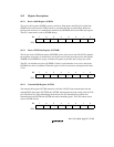
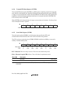
Lower 8 bits:76543210
ER TEND TDFE BRK FER PER RDF DR
Initial value:01100000
R/W: R/(W)
*
R/(W)
*
R/(W)
*
R/(W)
*
RRR/(W)
*
R/(W)
*
Note: * The only value that can be written is 0 to clear the flag.


