Rev. 5.00, 09/03, page 569 of 760
18.2 Register Configuration
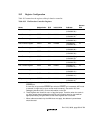
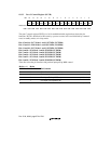
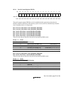
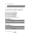
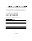
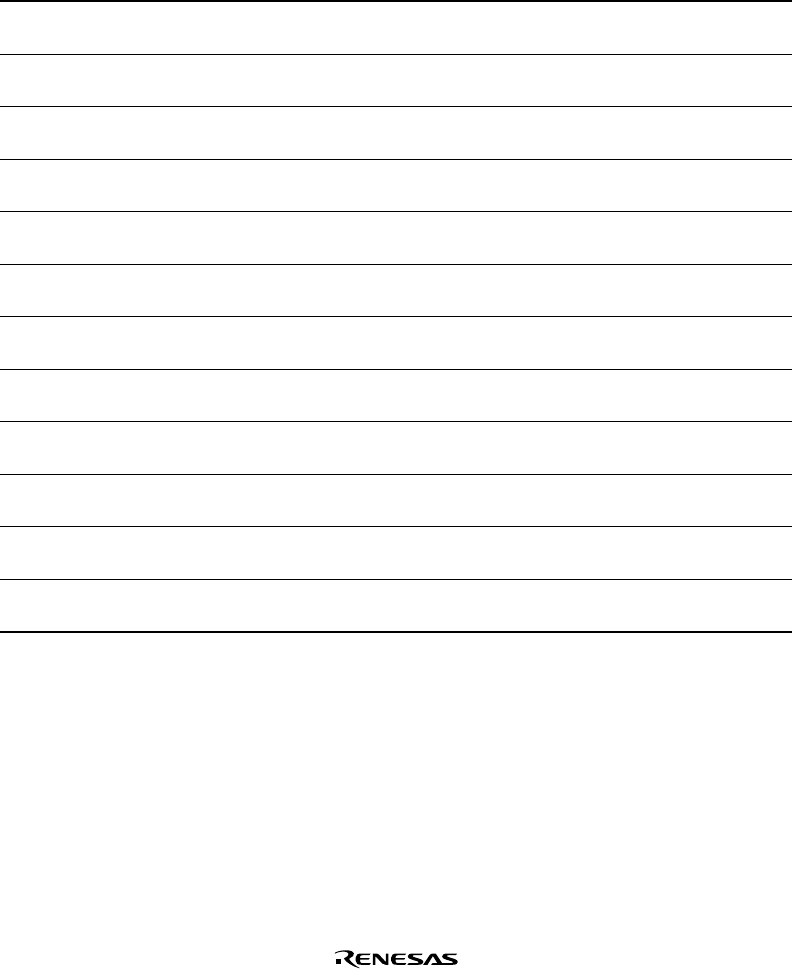
Table 18.2 summarizes the registers of the pin function controller.
Table 18.2 Pin Function Controller Registers
Name Abbreviation R/W Initial Value Address
Access
Size
Port A control register PACR R/W H'0000 H'04000100
(H'A4000100)
*
16
Port B control register PBCR R/W H'0000 H'04000102
(H'A4000102)
*
16
Port C control register PCCR R/W H'AAAA H'04000104
(H'A4000104)
*
16
Port D control register PDCR R/W H'AA8A H'04000106
(H'A4000106)
*
16
Port E control register PECR R/W H'AAAA/H'2AA8 H'04000108
(H'A4000108)
*
16
Port F control register PFCR R/W H'AAAA/H'00AA H'0400010A
(H'A400010A)
*
16
Port G control register PGCR R/W H'AAAA/H'A200 H'0400010C
(H'A400010C)
*
16
Port H control register PHCR R/W H'AAAA/H'8AAA H'0400010E
(H'A400010E)
*
16
Port J control register PJCR R/W H'0000 H'04000110
(H'A4000110)
*
16
Port K control register PKCR R/W H'0000 H'04000112
(H'A4000112)
*
16
Port L control register PLCR R/W H'0000 H'04000114
(H'A4000114)
*
16
SC port control register SCPCR R/W H'A888 H'04000116
(H'A4000116)
*
16
Notes: 1. The initial value of the port E, F, G, and H control registers depends on the state of the
ASEMD0 pin.
If a low level is input at the ASEMD0 pin while the RESETP pin is asserted, ASE mode
is entered; if a high level is input, normal mode is entered. See section 22, User
Debugging Interface (UDI), for more information on the UDI.
2. These registers are located in area 1 of physical space. Therefore, when the cache is
on, either access these registers from the P2 area of logical space or else make an
appropriate setting using the MMU so that these registers are not cached.
* When address translation by the MMU does not apply, the address in parentheses
should be used.


