Rev. 5.00, 09/03, page 475 of 760
Clock: An internal clock generated by the on-chip baud rate generator or an external clock input
from the SCK pin can be selected as the SCI transmit/receive clock. The clock source is selected
by the C/A bit in the serial mode register (SCSMR) and bits CKE1 and CKE0 in the serial control
register (SCSCR). See table 14.10.
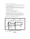
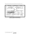
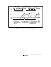
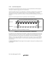
When the SCI operates on an internal clock, it outputs the clock signal at the SCK pin. Eight clock
pulses are output per transmitted or received character. When the SCI is not transmitting or
receiving, the clock signal remains in the high state. When only receiving, the SCI receives in 2-
character units, so a 16-pulse serial clock is output. To receive in 1-character units, select an
external clock source.
Transmitting and Receiving Data SCI Initialization (Synchronous Mode): Before
transmitting, receiving, or changing the mode or communication format, the software must clear
the TE and RE bits to 0 in the serial control register (SCSCR), then initialize the SCI. Clearing TE
to 0 sets TDRE to 1 and initializes the transmit shift register (SCTSR). Clearing RE to 0, however,
does not initialize the RDRF, PER, FER, and ORER flags and receive data register (SCRDR),
which retain their previous contents.
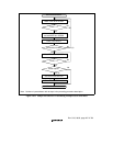
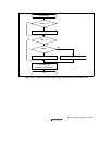
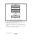
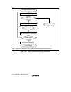
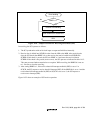
Figure 14.18 shows a sample flowchart for initializing the SCI. The procedure for initializing the
SCI is:
1. Select the clock source in the serial control register (SCSCR). Leave RIE, TIE, TEIE, MPIE,
TE and RE cleared to 0.
2. Select transmit/receive format in the serial mode register (SCSMR).
3. Write the value corresponding to the bit rate in the bit rate register (SCBRR) (not necessary if
an external clock is used).
4. Wait for at least the interval required to transmit or receive one bit, then set TE or RE in the
serial control register (SCSCR) to 1. Also set RIE, TIE, TEIE and MPIE. Setting TE and RE
allows use of the TxD and RxD pins.


