Rev. 5.00, 09/03, page 712 of 760
23.3.11 Delay Time Variation Due to Load Capacitance
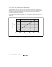
A graph (reference data) of the variation in delay time when a load capacitance greater than that
stipulated (30 or 50 pF) is connected to this LSI's pins is shown below. The graph shown in figure
23.60 should be taken into consideration in the design process if the stipulated capacitance is
exceeded in connecting an external device.
If the connected load capacitance exceeds the range shown in figure 23.60, the graph will not be a
straight line.
+3
+2
+1
+0
+0 +10 +20 +30 +40 +50
Load Capacitance [pF]
Delay Time [ns]
Figure 23.60 Load Capacitance vs. Delay Time


