Rev. 5.00, 09/03, page 231 of 760
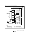
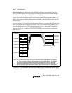
Area 0: H'00000000
Area 1: H'04000000
Area 2: H'08000000
A
rea 3: H'0C000000
Area 4: H'10000000
Area 5: H'14000000
The PCMCIA interface is shared
by the memory and I/O card
The PCMCIA interface is shared
by the memory and I/O card
Area 6: H'18000000
Ordinary memory/
burst ROM
Internal I/O
Ordinary memory/
synchronous DRAM
Ordinary memory/
synchronous DRAM
Ordinary memory
Ordinary memory/
burst ROM/PCMCIA
Ordinary memory/
burst ROM/PCMCIA
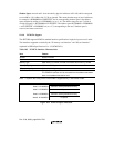
Figure 10.3 Physical Space Allocation
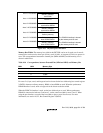
Memory Bus Width: The memory bus width in the SH7709S can be set for each area. In area 0,
external pins can be used to select byte (8 bits), word (16 bits), or longword (32 bits) on power-on
reset. The correspondence between the external pins (MD4 and MD3) and the memory size is
shown in table below.
Table 10.4 Correspondence between External Pins (MD4 and MD3) and Memory Size
MD4 MD3 Memory Size
0 0 Reserved (Do not set)
018 bits
1 0 16 bits
1 1 32 bits
For areas 2–6, byte, word, and longword can be chosen for the bus width using bus control register
2 (BCR2) whenever ordinary memory, ROM, or burst ROM are used. When the synchronous
DRAM interface is used, word or longword can be chosen as the bus width.
When the PCMCIA interface is used, set the bus width to byte or word. When synchronous
DRAM is connected to both area 2 and area 3, set the same bus width for areas 2 and 3. When
using the port function, set each of the bus widths to byte or word for all areas. For more
information, see section 10.2.2, Bus Control Register 2 (BCR2).


