Rev. 5.00, 09/03, page 223 of 760
Section 10 Bus State Controller (BSC)
10.1 Overview
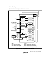
The bus state controller (BSC) divides physical address space and output control signals for
various types of memory and bus interface specifications. BSC functions enable the chip to link
directly with synchronous DRAM, SRAM, ROM, and other memory storage devices without an
external circuit. The BSC also allows direct connection to PCMCIA interfaces, simplifying system
design and allowing high-speed data transfers in a compact system.
10.1.1 Features
The BSC has the following features:
• Physical address space is divided into six areas
A maximum 64 Mbytes for each of the six areas, 0, 2–6
Area bus width can be selected by register (area 0 is set by external pin)
Wait states can be inserted using the WAIT pin
Wait state insertion can be controlled through software. Register settings can be used to
specify the insertion of 1–10 cycles independently for each area (1–38 cycles for areas 5
and 6 and the PCMCIA interface only)
The type of memory connected can be specified for each area, and control signals are
output for direct memory connection
Wait cycles are automatically inserted to avoid data bus conflict for continuous memory
accesses to different areas or writes directly following reads in the same area
• Direct interface to synchronous DRAM
Multiplexes row/column addresses according to synchronous DRAM capacity
Supports burst operation
Supports bank active mode
Has both auto-refresh and self-refresh functions
Controls timing of synchronous DRAM direct-connection control signals according to
register setting
• Burst ROM interface
Insertion of wait states controllable through software
Register setting control of burst transfers
• PCMCIA direct-connection interface
Insertion of wait states controllable through software
Bus sizing function for I/O bus width (only in little-endian mode)


