Rev. 5.00, 09/03, page 309 of 760
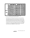
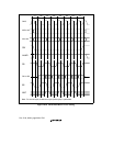
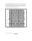
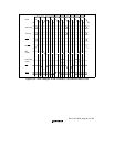
Memory Card Interface Basic Timing: Figure 10.32 shows the basic timing for the PCMCIA IC
memory card interface. When physical space areas 5 and 6 are designated as PCMCIA interface
areas, bus accesses are automatically performed as IC memory card interface accesses.
With a high external bus frequency (CKIO), the setup and hold times for the address (A24–A0),
card enable (CS5, CE2A, CS6, CE2B), and write data (D15–D0) in a write cycle, become
insufficient with respect to RD and WR (the WE pin in the SH7709S). The SH7709S provides for
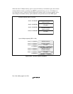
this by enabling setup and hold times to be set for physical space areas 5 and 6 in the PCR register.
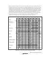
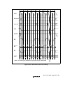
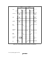
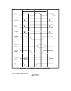
Also, software waits by means of a WCR2 register setting and hardware waits by means of the
WAIT pin can be inserted in the same way as for the basic interface. Figure 10.33 shows the
PCMCIA memory bus wait timing.


