Rev. 5.00, 09/03, page 662 of 760
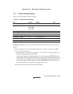
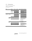
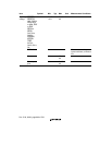
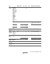
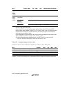
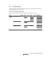
Item Symbol Min Typ Max Unit Measurement Conditions
Analog
power-
supply
voltage
AVcc 3.0 3.3 3.6 V
Analog
power-
supply
During A/D
conversion
AIcc — 0.8 2 mA
current During A/D
and D/A
conversion
—2.46 mA
Idle — 1 20 µA Ta = 25°C
Notes: Even when PLL is not used, always connect Vcc-PLL1 and Vcc-PLL2 to Vcc and connect
Vss-PLL1 and Vss-PLL2 to Vss.
Even when RTC is not used, always supply power between Vcc-RTC and Vss-RTC.
AVcc must be under condition of VccQ – 0.3 V ≤ AVcc ≤ VccQ + 0.3 V. If the A/D and D/A
converters are not used, do not leave the AVcc and AVss pins open. Connect AVcc to
VccQ, and connect AVss to VssQ.
Current dissipation values shown are the values at which all output pins are without load
under conditions of V
IH
min = VccQ – 0.5 V, V
IL
max = 0.5 V.
The same voltage should be supplied to Vcc, Vcc-RTC, Vcc-PLL1, and Vcc-PLL2.
* If the IRL and IRLS interrupts are used, the minimum is 1.9 V.
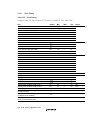
Table 23.3 Permitted Output Current Values
VccQ = 3.3 ± 0.3 V, Vcc = 1.55 to 2.15 V, AVcc = 3.3 ± 0.3 V, Ta = –20 to 75°C
Item Symbol Min Typ Max Unit
Output low-level permissible current (per pin) I
OL
——2.0mA
Output low-level permissible current (total) ∑ I
OL
— — 120 mA
Output high-level permissible current (per pin) –I
OH
——2.0mA
Output high-level permissible current (total) ∑ (–I
OH
)——40mA
Caution: To ensure LSI reliability, do not exceed the value for output current given in table 23.3.


