Rev. 5.00, 09/03, page 583 of 760
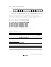
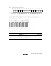
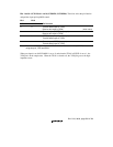
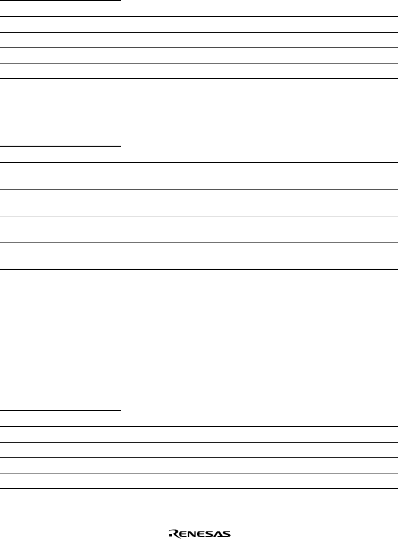
Bits 11 and 10—SCP5 Mode 1 and 0 (SCP5MD1, SCP5MD0): These bits select the pin
functions and perform input pull-up MOS control.
Bit 11 Bit 10
SCP5MD1 SCP5MD0 Pin Function
0 0 Other function (see table 18.1)
0 1 Port output
1 0 Port input (Pull-up MOS: on) (Initial value)
1 1 Port input (Pull-up MOS: off)
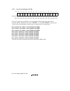
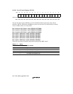
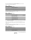
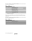
Bits 9 and 8—SCP4 Mode 1 and 0 (SCP4MD1, SCP4MD0): These bits select the pin function
and perform input pull-up MOS control.
Bit 9 Bit 8
SCP4MD1 SCP4MD0 Pin Function
0 0 Transmit data output 2 (TxD2)
Receive data input 2 (RxD2) (Initial value)
0 1 General output (SCPT[4] output pin)
Receive data input 2 (RxD2)
1 0 SCPT[4] input pin pull-up (input pin)
Transmit data output 2 (TxD2)
1 1 General input (SCPT[4] input pin)
Transmit data output 2 (TxD2)
Note: There is no SCPT[4] simultaneous I/O combination because one bit (SCP4DT) is accessed
using two pins, TxD2 and RxD2.
When port input is set (bit SCPnMD1 is set to 1) and when the TE bit in SCSCR is set to 1, the
TxD2 pin is in the output state. When the TE bit is cleared to 0, the TxD2 pin goes to the high-
impedance state.
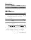
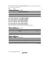
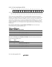
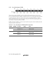
Bits 7 and 6—SCP3 Mode 1 and 0 (SCP3MD1, SCP3MD0): These bits select the pin function
and perform input pull-up MOS control.
Bit 7 Bit 6
SCP3MD1 SCP3MD0 Pin Function
0 0 Other function (see table 18.1)
0 1 Port output
1 0 Port input (Pull-up MOS: on) (Initial value)
1 1 Port input (Pull-up MOS: off)


