Rev. 5.00, 09/03, page 641 of 760
Section 22 User Debugging Interface
(UDI)
22.1 Overview
This LSI incorporates a User debugging interface (UDI) and advanced user debugger (AUD) for
program debugging.
22.2 User Debugging Interface (UDI)
The UDI (User debugging interface) performs on-chip debugging which is supported by this LSI.
The UDI described here is a serial interface which is compatible with JTAG (Joint Test Action
Group, IEEE Standard 1149.1 and IEEE Standard Test Access Port and Boundary-Scan
Architecture) specifications.
The UDI in the SH7709S supports a boundary scan mode, and is also used for emulator
connection.
When using an emulator, UDI functions should not be used. Refer to the emulator manual for the
method of connecting the emulator.
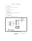
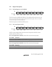
22.2.1 Pin Descriptions
TCK: UDI serial data input/output clock pin. Data is serially supplied to the UDI from the data
input pin (TDI), and output from the data output pin (TDO), in synchronization with this clock.
TMS: Mode select input pin. The state of the TAP control circuit is determined by changing this
signal in synchronization with TCK. The protocol complies with the JTAG standard (IEEE Std.
1149.1).
T
TT
TR
RR
RS
SS
ST
TT
T: UDI reset input pin. Input is accepted asynchronously with respect to TCK, and when low,
the UDI is reset. See section 22.4.2, Reset Configuration, for more information.
TDI: UDI serial data input pin. Data transfer to the UDI is executed by changing this signal in
synchronization with TCK.
TDO: UDI serial data output pin. Data output from the UDI is executed by reading this signal in
synchronization with TCK.
A
AA
AS
SS
SE
EE
EM
MM
MD
DD
D0
00
0: ASE mode select pin. If a low level is input at the ASEMD0 pin while the RE SETP
pin is asserted, ASE mode is entered; if a high level is input, normal mode is entered. When using
on the user system alone, without an emulator and the UDI, hold this pin at high level. In ASE


