Rev. 5.00, 09/03, page 636 of 760
21.1.3 I/O Pins
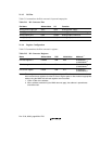
Table 21.1 summarizes the D/A converter’s input and output pins.
Table 21.1 D/A Converter Pins
Pin Name Abbreviation I/O Function
Analog power supply pin AVcc Input Analog power supply
Analog ground pin AVss Input Analog ground and reference voltage
Analog output pin 0 DA0 Output Analog output, channel 0
Analog output pin 1 DA1 Output Analog output, channel 1
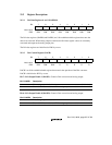
21.1.4 Register Configuration
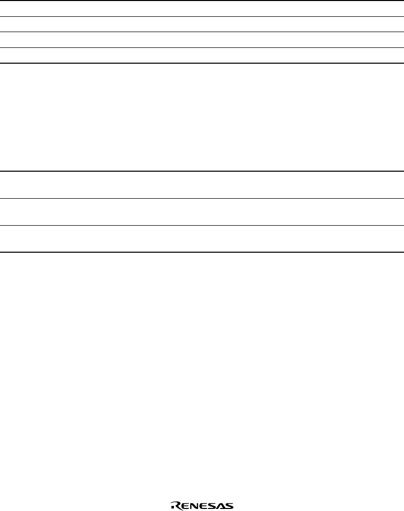
Table 21.2 summarizes the D/A converter’s registers.
Table 21.2 D/A Converter Registers
Name Abbreviation R/W Initial Value Address
*
1
D/A data register 0 DADR0 R/W H'00 H'040000A0
(H'A40000A0)
*
2
D/A data register 1 DADR1 R/W H'00 H'040000A2
(H'A40000A2)
*
2
D/A control register DACR R/W H'1F H'040000A4
(H'A40000A4)
*
2
Notes: These registers are located in area 1 of physical space. Therefore, when the cache is on,
either access these registers from the P2 area of logical space or else make an appropriate
setting using the MMU so that these registers are not cached.
1. Lower 16 bits of the address
2. When address translation by the MMU does not apply, the address in parentheses
should be used.


