Rev. 5.00, 09/03, page 282 of 760
independently for areas 2 and 3 by means of bits A2W1 and A2W0 or A3W1 and A3W0 in
WCR2. This number of cycles corresponds to the number of synchronous DRAM CAS latency
cycles.
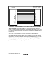
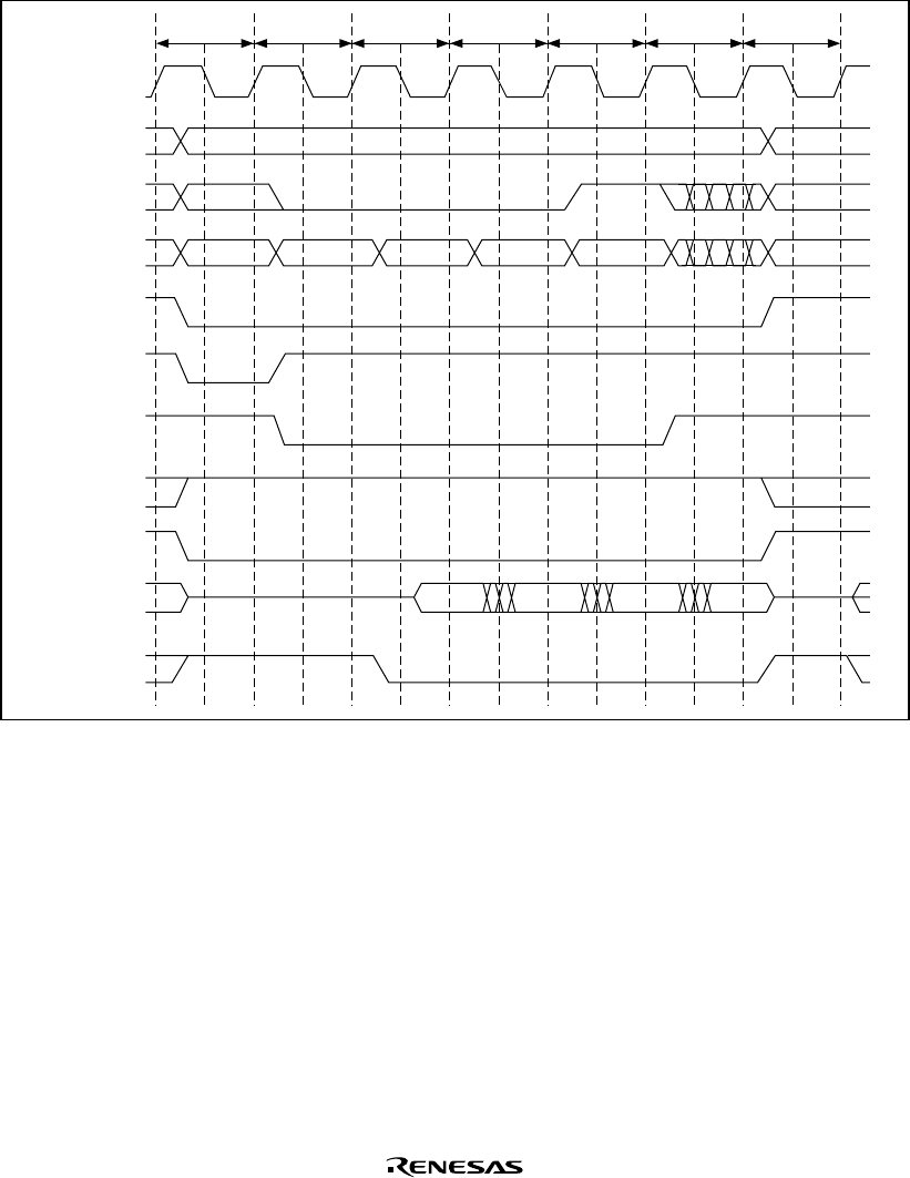
CKIO
A
25 to A16,
A
13
A
12
A
15, A14,
A
11 to A0
CS2 or CS3
RAS3x
CASx
RD/WR
DQMxx
D31 to D0
BS
Tr Tc1 Tc2/Td1 Tc3/Td2 Tc4/Td3 Td4 Tpc
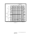
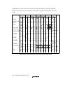
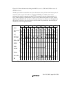
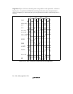
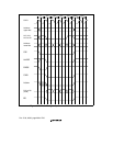
Figure 10.14 Basic Timing for Synchronous DRAM Burst Read


