Rev. 5.00, 09/03, page 185 of 760
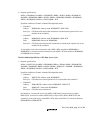
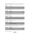
Bit 0—Module Standby 0 (MSTP0): Specifies halting of the clock supply to the serial
communication interface SCI (an on-chip peripheral module). When the MSTP0 bit is set to 1, the
supply of the clock to the SCI is halted.
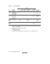
Bit 0: MSTP0 Description
0 SCI operates (Initial value)
1 Clock supply to SCI is halted
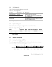
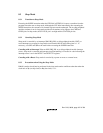
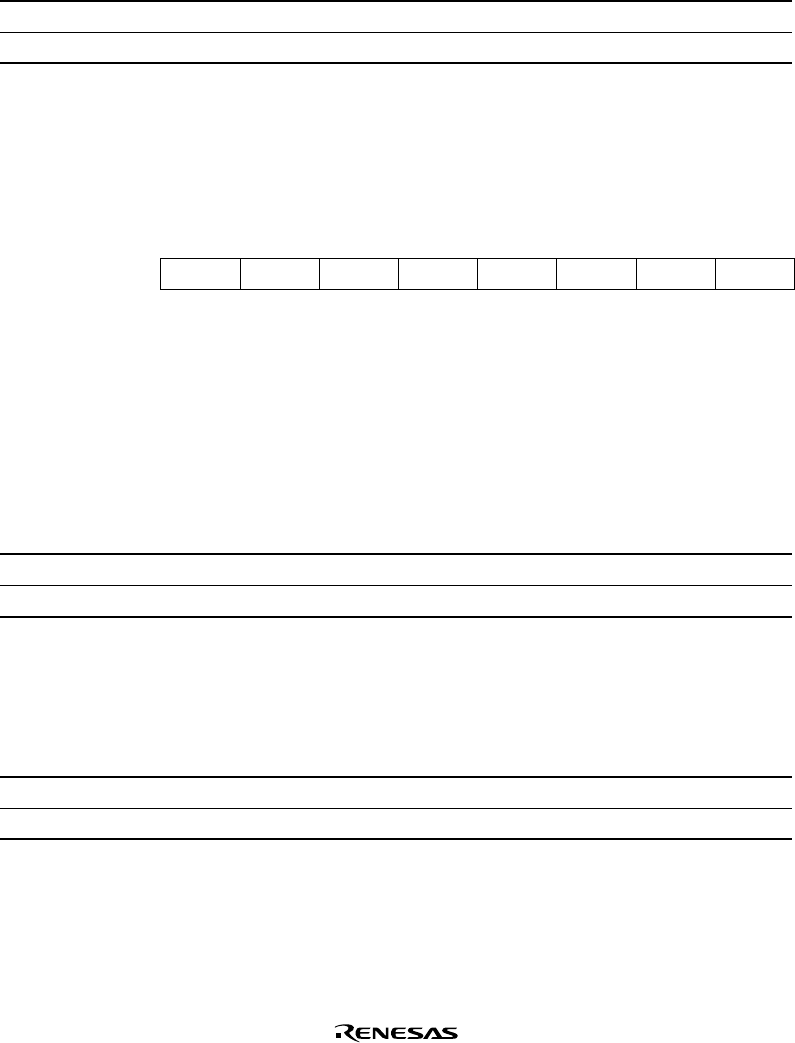
8.2.2 Standby Control Register 2 (STBCR2)
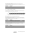
The standby control register 2 (STBCR2) is a readable/writable 8-bit register that sets the power-
down mode. STBCR2 is initialized to H'00 by a power-on reset.
Bit:76543210
MDCHG MSTP8 MSTP7 MSTP6 MSTP5 MSTP4 MSTP3
Initial value:00000000
R/W: R/W R/W R/W R/W R/W R/W R/W R/W
Bit 7—Reserved: The write value set in the program should always be 1.
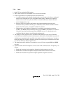
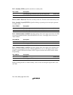
Bit 6—Pin MD5 to MD0 Control (MDCHG): Specifies whether or not pins MD5 to MD0 are
changed in standby mode. When this bit is set to 1, the MD5 to MD0 pin values are latched when
returning from standby mode by means of a reset or interrupt.
Bit 6: MDCHG Description
0 Pins MD5 to MD0 are not changed in standby mode (Initial value)
1 Pins MD5 to MD0 are changed in standby mode
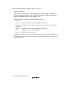
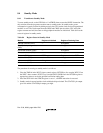
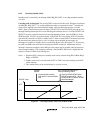
Bit 5— Module Stop 8 (MSTP8): Specifies halting of the clock supply to the user break
controller UBC (an on-chip peripheral module). When the MSTP8 bit is set to 1, the supply of the
clock to the UBC is halted.
Bit 5: MSTP8 Description
0 UBC runs (Initial value)
1 Clock supply to UBC is halted


