Rev. 5.00, 09/03, page 106 of 760
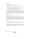
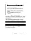
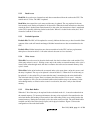
CEWTCF CB
012345631
………………… …
: Reserved bits. Always 0 when reading. Data written here is also always 0.
CF: Cache flush bit. Writing 1 flushes all cache entries (clears the V, U, and LRU bits of all
cache entries to 0). Always reads 0. Write-back to external memory is not performed when
the cache is flushed.
CB: Write-back/write-through switchover bit. Indicates the cache’s operating mode for area P1.
1 = write-back mode, 0 = write-through mode.
WT: Write-through bit. Indicates the cache’s operating mode for area P0, U0, and P3.
1 = write-through mode, 0 = write-back mode.
CE: Cache enable bit. Indicates whether the cache function is used.
1 = cache used, 0 = cache not used.
Figure 5.2 CCR Register Configuration
5.2.2 Cache Control Register 2 (CCR2)
CCR2 is used to control the cache-lock function and is valid only in cache locking mode. Cache
locking mode means that the cache lock bit (bit 12) in SR (status register) is set to 1. The cache-
lock function is invalid in non-cache locking mode (the cache-lock bit is 0).
When a prefetch instruction (PREF) is executed in cache locking mode and a cache miss occurs,
one line size of data pointed to by Rn is brought to cache according to the setting of bits 9 and 8
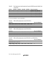
(W3LOAD and W3LOCK) and bits 1 and 0 (W2LOAD and W2LOCK) in CCR2. Table 5.4
shows the relationship between the bit setting and way to be replaced when a prefetch instruction
is executed. When a prefetch instruction is executed and there is a cache hit, new data is not
fetched and an entry which has already been valid is retained. For example, when the cache-lock,
W3LOAD, and W3LOCK bits are set to 1 and a prefetch instruction is executed while one line
size of data pointed to by Rn is already in way 0, a cache hit occurs and data is not fetched to way
3.
When cache is accessed by means of instructions except for a prefetch instruction in cache locking
mode, a way that is replaced by the W3LOCK and W2LOCK bits is restricted. Table 5.5 shows
the relationship between the bit setting of CCR2 and way to be replaced.
The program which modifies the contents of CCR2 must be placed in an address space which does
not cache.
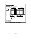
Figure 5.3 shows the configuration of CCR2.
CCR2 is a write-only register; if read, an undefined value will be returned.


