Rev. 5.00, 09/03, page 332 of 760
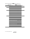
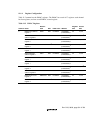
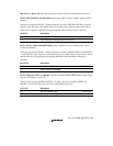
Channel Name
Abbrevi-
ation R/W Initial Value Address
Register
Size
Access
Size
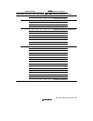
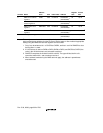
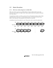
3 DMA source address
register 3
SAR3 R/W Undefined H'04000050
(H'A4000050)
*
4
32 16, 32
*
2
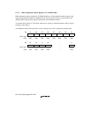
DMA destination
address register 3
DAR3 R/W Undefined H'04000054
(H'A4000054)
*
4
32 16, 32
*
2
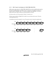
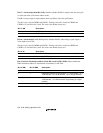
DMA transfer count
register 3
DMATCR3 R/W Undefined H'04000058
(H'A4000058)
*
4
24 16, 32
*
3
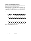
DMA channel control
register 3
CHCR3 R/W
*
1
H'00000000 H'0400005C
(H'A400005C)
*
4
32 8, 16, 32
*
2
Shared DMA operation register DMAOR R/W
*
1
H'0000 H'04000060
(H'A4000060)
*
4
16 8, 16
*
2
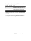
Notes: These registers are located in area 1 of physical space. Therefore, when the cache is on,
either access these registers from the P2 area of logical space or else make an appropriate
setting using the MMU so that these registers are not cached.
1. Only 0 can be written to bit 1 of CHCR0 to CHCR3, and bits 1 and 2 of DMAOR to clear
the flag after 1 is read.
2. If 16-bit access is used on SAR0 to SAR3, DAR0 to DAR3, and CHCR0 to CHCR3, the
value in the 16 bits that were not accessed is retained.
3. DMATCR comprises the 24 bits from bit 0 to bit 23. The upper 8 bits, bits 24 to 31,
cannot be written with 1 and are always read as 0.
4. When address translation by the MMU does not apply, the address in parentheses
should be used.


