Rev. 5.00, 09/03, page 226 of 760
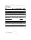
10.1.3 Pin Configuration
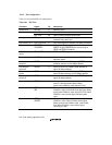
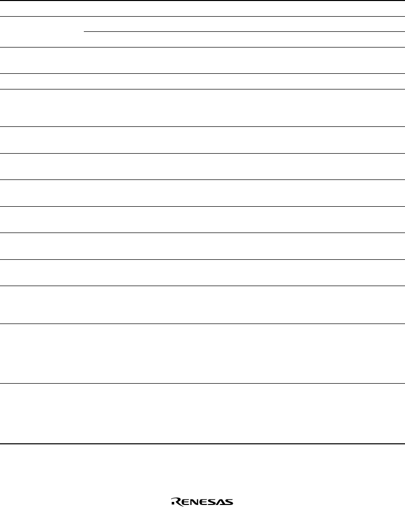
Table 10.1 shows the BSC pin configuration.
Table 10.1 BSC Pins
Pin Name Signal I/O Description
Address bus A25–A0 O Address output
Data bus D15–D0 I/O Data I/O
D31–D16 I/O Data I/O when using 32-bit bus width
Bus cycle start BS O Shows start of bus cycle. During burst transfers,
asserted every data cycle.
Chip select 0, 2–4 CS0, CS2–CS4 O Chip select signals to indicate area being accessed.
Chip select 5, 6 CS5/CE1A,
CS6/CE1B
O Chip select signals to indicate area being accessed.
CS5/CE1A and CS6/CE1B can also be used as
CE1A and CE1B of PCMCIA.
PCMCIA card
select
CE2A, CE2B O CE2A and CE2B signals when PCMCIA is used
Read/write RD/WR O Data bus direction indication signal. PCMCIA write
indication signal.
Row address
strobe 3L
RAS3L O When synchronous DRAM is used, RAS3L for lower
32-Mbyte address and 64-Mbyte address.
Row address
strobe 3U
RAS3U O When synchronous DRAM is used, RAS3U for
upper 32-Mbyte address.
Column address
strobe
CASL O When synchronous DRAM is used, CASL signal for
lower 32-Mbyte address and 64-Mbyte address.
Column address
strobe LH
CASU O When synchronous DRAM is used, CASU signal for
upper 32-Mbyte address.
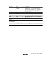
Data enable 0 WE0/DQMLL O When memory other than synchronous DRAM is
used, D7–D0 write strobe signal. When
synchronous DRAM is used, selects D7–D0.
Data enable 1 WE1/DQMLU/
WE
O When memory other than synchronous DRAM and
PCMCIA is used, D15–D8 write strobe signal. When
synchronous DRAM is used, selects D15–D8. When
PCMCIA is used, strobe signal indicating write
cycle.
Data enable 2 WE2/DQMUL/
ICIORD
O When memory other than synchronous DRAM and
PCMCIA is used, D23–D16 write strobe signal.
When synchronous DRAM is used, selects D23–
D16. When PCMCIA is used, strobe signal
indicating I/O read.


