Rev. 5.00, 09/03, page 642 of 760
mode, boundary scan and emulator functions can be used. The input level at the ASEMD0 pin
should be held for at least one cycle after RESETP negation.
A
AA
AS
SS
SE
EE
EB
BB
BR
RR
RKAK
KAKKAK
KAK: Dedicated emulator pin
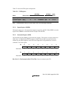
22.2.2 Block Diagram
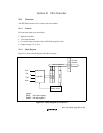
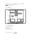
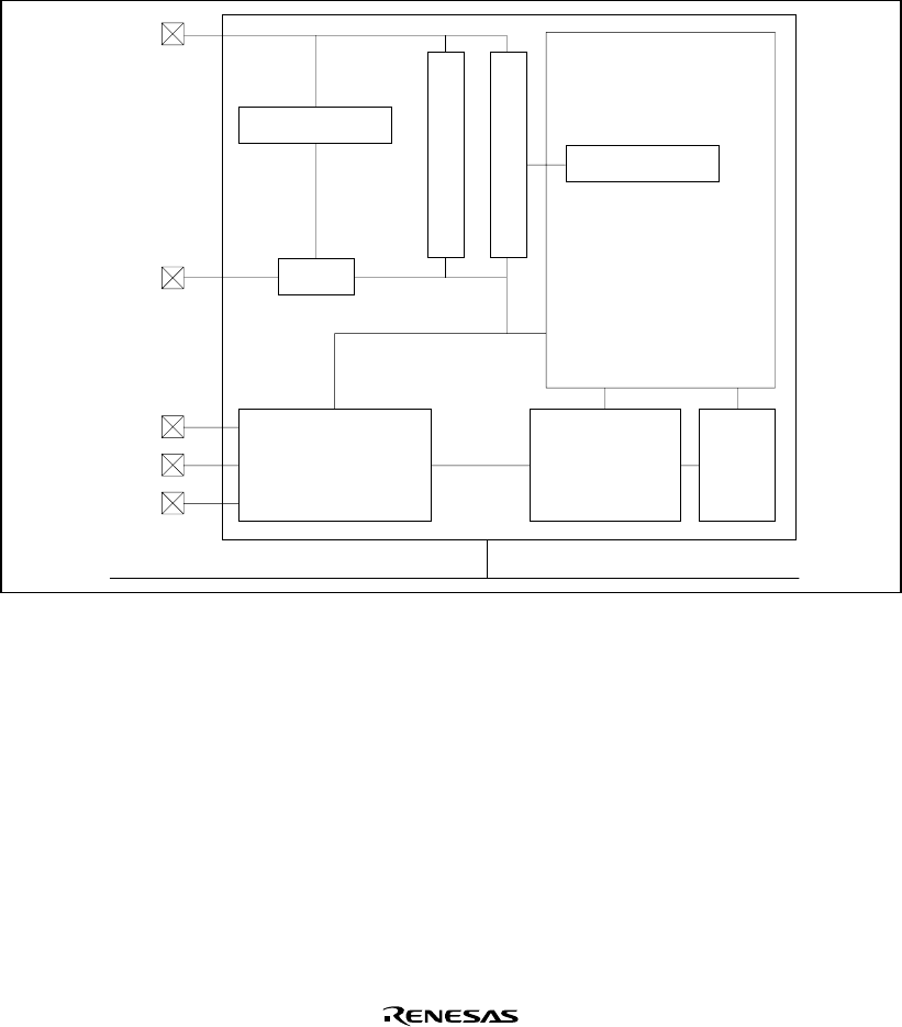
Figure 22.1 shows a block diagram of the UDI.
SDIR
TCK
TDO
TDI
TMS
TRST
SDBPR
MUX
SDBSR
Shift register
TAP controller
Decoder
Local
bus
Figure 22.1 Block Diagram of UDI
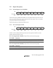
22.3 Register Descriptions
The UDI has the following registers.
• SDBPR: Bypass register
• SDIR: Instruction register
• SDBSR: Boundary scan register


