Rev. 5.00, 09/03, page 217 of 760
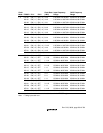
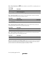
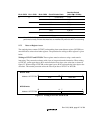
Bit 2: CKS2 Bit 1: CKS1 Bit 0: CKS0 Clock Division Ratio
Overflow Period
(when Pφ
φφ
φ = 15 MHz)
0001(Initial value)17 µs
1 1/4 68 µs
1 0 1/16 273 µs
1 1/32 546 µs
1001/64 1.09 ms
1 1/256 4.36 ms
1 0 1/1024 17.48 ms
1 1/4096 69.91 ms
Note: If bits CKS2–CKS0 are modified when the WDT is running, the up-count may not be
performed correctly. Ensure that these bits are modified only when the WDT is not running.
9.7.3 Notes on Register Access
The watchdog timer counter (WTCNT) and watchdog timer control/status register (WTCSR) are
more difficult to write to than other registers. The procedure for writing to these registers is given
below.
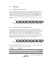
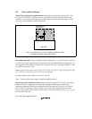
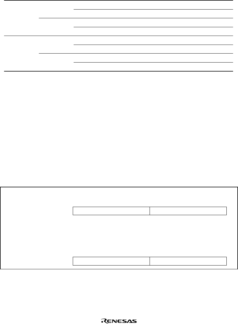
Writing to WTCNT and WTCSR: These registers must be written to using a word transfer
instruction. They cannot be written to with a byte or longword transfer instruction. When writing
to WTCNT, set the upper byte to H'5A and transfer the lower byte as the write data, as shown in
figure 9.3. When writing to WTCSR, set the upper byte to H'A5 and transfer the lower byte as the
write data. This transfer procedure writes the lower byte data to WTCNT or WTCSR.
15 8 7 0
H'5A Write data
Address: H'FFFFFF84
WTCNT write
15 8 7 0
H'A5 Write data
Address: H'FFFFFF86
WTCSR write
Figure 9.3 Writing to WTCNT and WTCSR


