Rev. 5.00, 09/03, page 616 of 760
20.1.4 Register Configuration
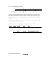
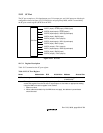
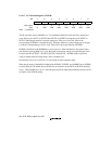
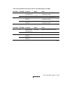
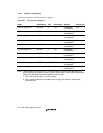
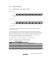
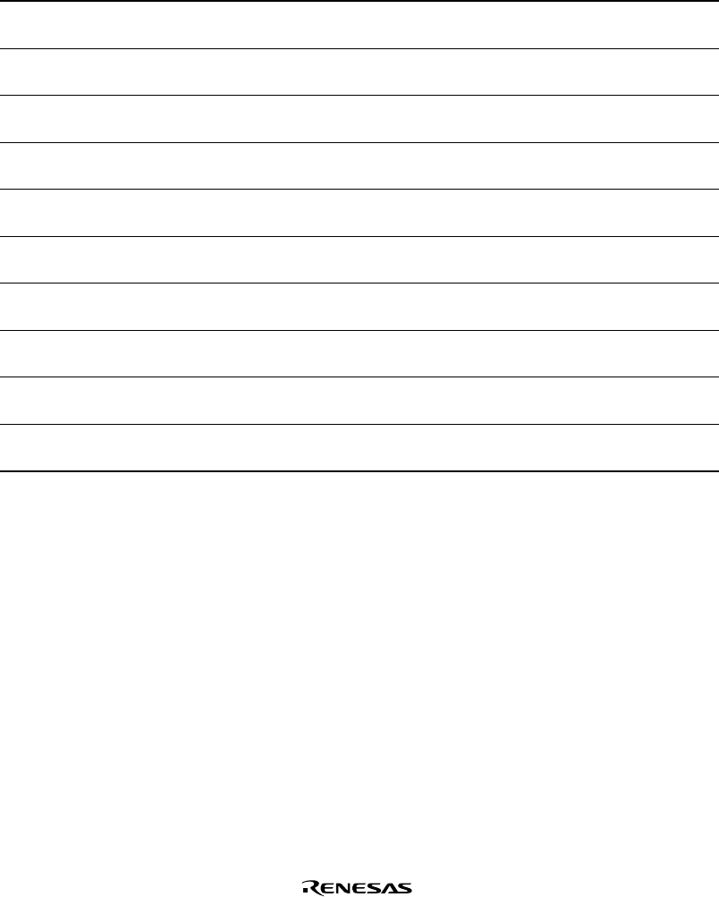
Table 20.2 summarizes the A/D converter’s registers.
Table 20.2 A/D Converter Registers
Name Abbreviation R/W Initial Value Address Access size
A/D data register AH ADDRAH R H'00 H'04000080
(H'A4000080)
*
2
16, 8
A/D data register AL ADDRAL R H'00 H'04000082
(H'A4000082)
*
2
8
A/D data register BH ADDRBH R H'00 H'04000084
(H'A4000084)
*
2
16, 8
A/D data register BL ADDRBL R H'00 H'04000086
(H'A4000086)
*
2
8
A/D data register CH ADDRCH R H'00 H'04000088
(H'A4000088)
*
2
16, 8
A/D data register CL ADDRCL R H'00 H'0400008A
(H'A400008A)
*
2
8
A/D data register DH ADDRDH R H'00 H'0400008C
(H'A400008C)
*
2
16, 8
A/D data register DL ADDRDL R H'00 H'0400008E
(H'A400008E)
*
2
8
A/D control/status register ADCSR R/(W)
*
1
H'00 H'04000090
(H'A4000090)
*
2
8
A/D control register ADCR R/W H'07 H'04000092
(H'A4000092)
*
2
8
Notes: These registers are located in area 1 of physical space. Therefore, when the cache is on,
either access these registers from the P2 area of logical space or else make an appropriate
setting using the MMU so that these registers are not cached.
1. Only 0 can be written to bit 7, to clear the flag.
2. When address translation by the MMU does not apply, the address in parentheses
should be used.


