Rev. 5.00, 09/03, page 497 of 760
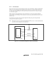
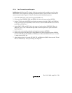
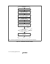
5. The transmitting side transmits the next frame of data unless it receives an error signal. If it
does receive an error signal, it returns to step 2 to re-transmit the erroneous data.
15.3.4 Register Settings
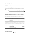
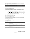
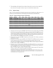
Table 15.3 shows the bit map of the registers that the smart card interface uses. Bits shown as 1 or
0 must be set to the indicated value. The settings for the other bits are described below.
Table 15.3 Register Settings for Smart Card Interface
Register Address Bit 7 Bit 6 Bit 5 Bit 4 Bit 3 Bit 2 Bit 1 Bit 0
SCSMR H'FFFFFE80 C/A 01O/E 1 0 CKS1 CKS0
SCBRR H'FFFFFE82 BRR7 BRR6 BRR5 BRR4 BRR3 BRR2 BRR1 BRR0
SCSCR H'FFFFFE84 TIE RIE TE RE 0 0 CKE1 CKE0
SCTDR H'FFFFFE86 TDR7 TDR6 TDR5 TDR4 TDR3 TDR2 TDR1 TDR0
SCSSR H'FFFFFE88 TDRE RDRF ORER FER/
ERS
PER TEND 0 0
SCRDR H'FFFFFE8A RDR7 RDR6 RDR5 RDR4 RDR3 RDR2 RDR1 RDR0
SCSCMR H'FFFFFE8C — ———SDIRSINV—SMIF
Note: Dashes indicate unused bits.
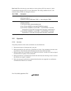
1. Setting the serial mode register (SCSMR): The C/A bit selects the setting timing of the TEND
flag, and selects the clock output state in combination with bits CKE1 and CKE0 in the serial
control register (SCSCR). Clear the O/E bit to 0 if the IC card uses the direct convention, and
set it to 1 if the card uses the inverse convention. Select the on-chip baud rate generator clock
source with the CKS1 and CKS0 bits (see section 15.3.5, Clock).
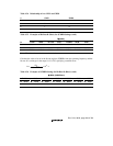
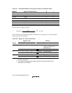
2. Setting the bit rate register (SCBRR): Set the bit rate. See section 15.3.5, Clock, to see how to
calculate the set value.
3. Setting the serial control register (SCSCR): The TIE, RIE, TE and RE bits function as they do
for the ordinary SCI. See section 14, Serial Communication Interface (SCI), for more
information. The CKE0 bit specifies the clock output. When no clock is output, clear CKE0 to
0; when a clock is output, set CKE0 to 1.
4. Setting the smart card mode register (SCSCMR): The SDIR and SINV bits are both cleared to
0 for IC cards that use the direct convention, and both set to 1 when the inverse convention is
used. The SMIF bit is set to 1 for the smart card interface.
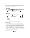
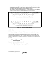
Figure 15.4 shows sample waveforms for register settings of the two types of IC cards (direct
convention and inverse convention) and their start characters.
In the direct convention type, the logical 1 level is state Z, the logical 0 level is state A, and
communication is LSB-first. The start character data is H'3B. Parity is even (from the smart
card standard), and so the parity bit is 1.


