Rev. 5.00, 09/03, page 86 of 760
contents of PC and SR to return to the processor state at the point of interruption and the address
where the exception occurred.
A basic exception handling sequence consists of the following operations:
1. The contents of PC and SR are saved in SPC and SSR, respectively.
2. The block (BL) bit in SR is set to 1, masking any subsequent exceptions.
3. The mode (MD) bit in SR is set to 1 to place the SH7709S in privileged mode.
4. The register bank (RB) bit in SR is set to 1.
5. An exception code identifying the exception event is written to bits 11–0 of the exception
event (EXPEVT) or interrupt event (INTEVT or INTEVT2) register.
6. Instruction execution jumps to the designated exception vector address to invoke the handler
routine.
4.2.2 Exception Vector Addresses
The reset vector address is fixed at H'A0000000. The other three events are assigned offsets from
the vector base address by software. Translation look-aside buffer (TLB) miss exceptions have an
offset from the vector base address of H'00000400. The vector address offset for general exception
events other than TLB miss exceptions is H'00000100. The interrupt vector address offset is
H'00000600. The vector base address is loaded into the vector base register (VBR) by software.
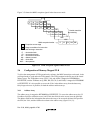
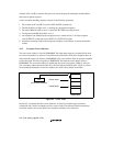
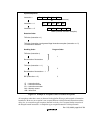
The vector base address should reside in P1 or P2 fixed physical address space. Figure 4.1 shows
the relationship between the vector base address, the vector offset, and the vector table.
VBR
(Vector base address)
+ Vector offset
H'A000 0000
Vector table
Figure 4.1 Vector Table
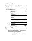
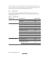
In table 4.2, exceptions and their vector addresses are listed by exception type, instruction
completion state, relative acceptance priority, relative order of occurrence within an instruction
execution sequence and vector address for exceptions and their vector addresses.


