Rev. 5.00, 09/03, page 617 of 760
20.2 Register Descriptions
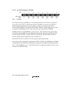
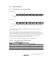
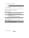
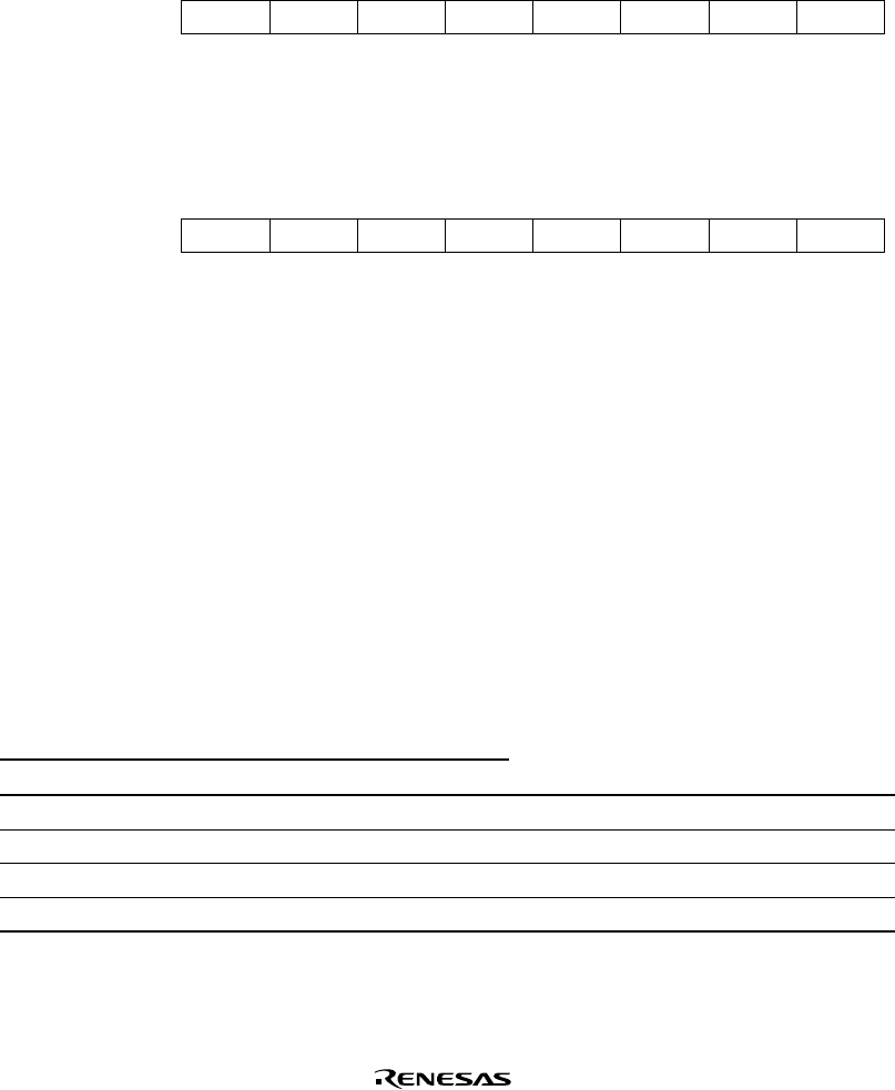
20.2.1 A/D Data Registers A to D (ADDRA to ADDRD)
Upper register: H
Bit:76543210
AD9 AD8 AD7 AD6 AD5 AD4 AD3 AD2
Initial value:00000000
R/W:RRRRRRRR
Lower register: L
Bit:76543210
AD1AD0——————
Initial value:00000000
R/W:RRRRRRRR
n = A to D
The four A/D data registers (ADDRA to ADDRD) are 16-bit read-only registers that store the
results of A/D conversion.
An A/D conversion produces 10-bit data, which is transferred for storage into the A/D data
register corresponding to the selected channel. The upper 8 bits of the result are stored in the upper
byte (bits 7 to 0) of the A/D data register. The lower 2 bits are stored in the lower byte (bits 7 and
6). Bits 5 to 0 of an A/D data register are reserved bits that are always read as 0. Table 20.3
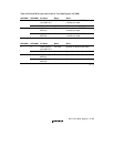
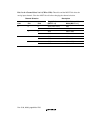
indicates the pairings of analog input channels and A/D data registers.
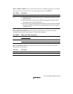
The A/D data registers are initialized to H'0000 by a reset and in standby mode.
Table 20.3 Analog Input Channels and A/D Data Registers
Analog Input Channel
Group 0 Group 1 A/D Data Register
AN0 AN4 ADDRA
AN1 AN5 ADDRB
AN2 AN6 ADDRC
AN3 AN7 ADDRD


