Rev. 5.00, 09/03, page 609 of 760
19.13 SC Port
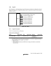
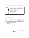
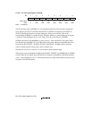
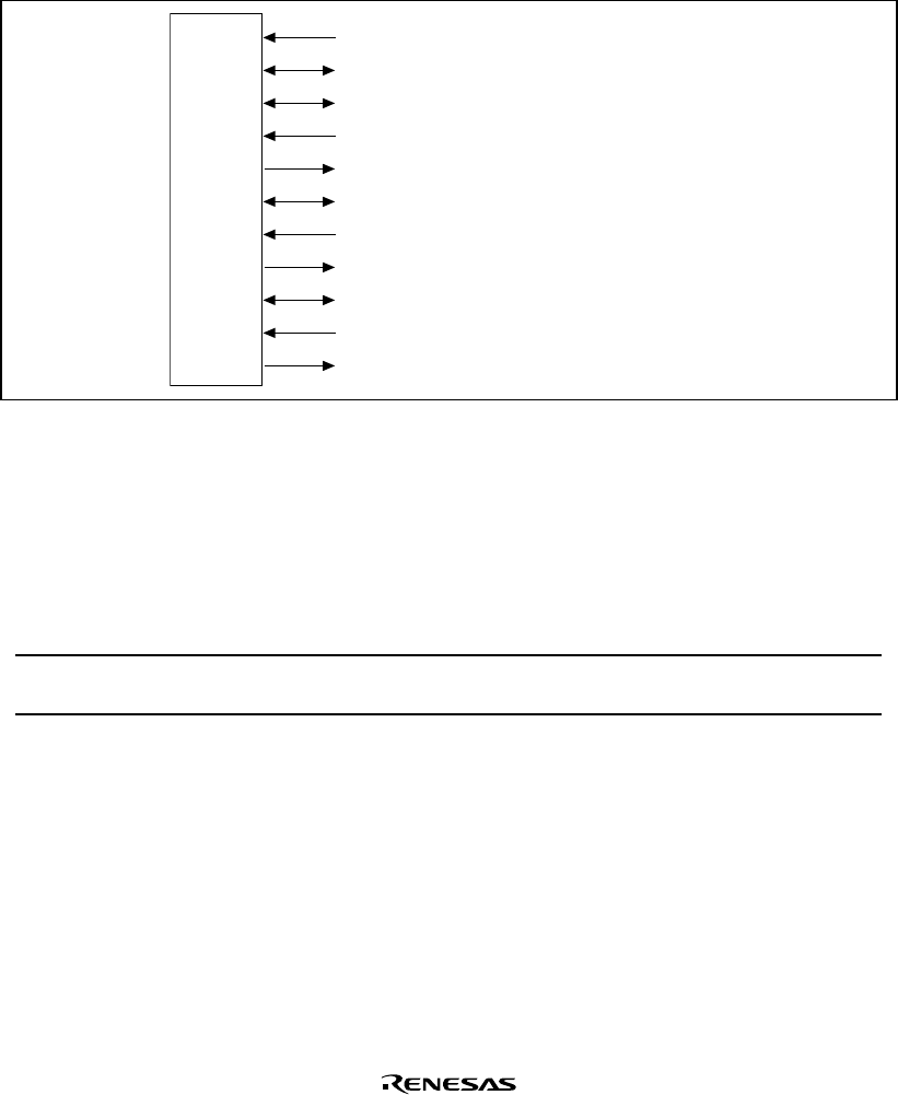
The SC port comprises a 4-bit input/output port, 3-bit output port, and 4-bit input port with the pin
configuration shown in figure 19.12. Each pin has an input pull-up MOS, which is controlled by
the SC port control register (SCPCR) in the PFC.
SCPT7 (input) / CTS2 (input) / IRQ5 (input)
SCPT6 (input/output) / RTS2 (output)
SCPT5 (input/output) / SCK2 (input/output)
SCPT4 (input) / RxD2 (input)
SCPT4 (output) / TxD2 (output)
SCPT3 (input/output) / SCK1 (input/output)
SCPT2 (input) / RxD1 (input)
SCPT2 (output) / TxD1 (output)
SCPT1 (input/output) / SCK0 (input/output)
SCPT0 (input) / RxD0 (input)
SCPT0 (output) / TxD0 (output)
SC Port
Figure 19.12 SC Port
19.13.1 Register Description
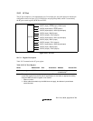
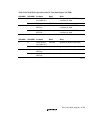
Table 19.23 summarizes the SC port register.
Table 19.23 SC Port Register
Name Abbreviation R/W Initial Value Address Access Size
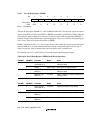
SC Port data register SCPDR R/W or R B'*0000000 H'04000136
(H'A4000136)
*
1
8
Notes: This register is located in area 1 of physical space. Therefore, when the cache is on, either
access this register from the P2 area of logical space or else make an appropriate setting
using the MMU so that this register is not cached.
* Means no value.
*1 When address translation by the MMU does not apply, the address in parentheses
should be used.


