Rev. 5.00, 09/03, page 268 of 760
10.3.3 Basic Interface
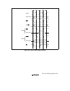
Basic Timing: The basic interface of the SH7709S uses strobe signal output in consideration of
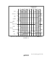
the fact that mainly static RAM will be directly connected. Figure 10.6 shows the basic timing of
normal space accesses. A no-wait normal access is completed in two cycles. The BS signal is
asserted for one cycle to indicate the start of a bus cycle. The CSn signal is negated on the T2
clock falling edge to secure the negation period. Therefore, in case of access at minimum pitch,
there is a half-cycle negation period.
There is no access size specification when reading. The correct access start address is output in the
least significant bit of the address, but since there is no access size specification, 32 bits are always
read in case of a 32-bit device, and 16 bits in case of a 16-bit device. When writing, only the WE
signal for the byte to be written is asserted. For details, see section 10.3.1, Endian/Access Size and
Data Alignment.
Read/write for cache fill or write-back follows the set bus width and transfers a total of 16 bytes
continuously. The bus is not released during this transfer. For cache misses that occur during byte
or word operand accesses or branching to odd word boundaries, the fill is always performed by
longword accesses on the chip-external interface. Write-through-area write access and non-
cacheable read/write access are based on the actual address size.


