Rev. 5.00, 09/03, page 594 of 760
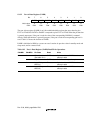
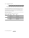
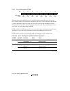
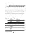
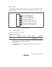
19.5.2 Port D Data Register (PDDR)
Bit:76543210
PD7DT PD6DT PD5DT PD4DT PD3DT PD2DT PD1DT PD0DT
Initial value: 0 * 0 * 0000
R/W: R/W R R/W R R/W R/W R/W R/W
Note: * Undefined
The port D data register (PDDR) is a 6-bit readable/writable and 2-bit read-only register that stores
data for pins PTD7 to PTD0. Bits PD7DT to PD0DT correspond to pins PTD7 to PTD0. When the
pin function is general output port, if the port is read, the value of the corresponding PDDR bit is
returned directly. When the function is general input port, if the port is read, the corresponding pin
level is read. Table 19.8 shows the function of PDDR.
PDDR is initialized to B'0*0*0000 by a power-on reset. After initialization, the general input port
function (pull-up MOS on) is set as the initial pin function, and the corresponding pin levels are
read from bits PD7DT—PD3DT, PD1DT, and PD0DT. PDDR retains its previous value in
standby mode and sleep mode, and in a manual reset.
Note that the low level is read if bits 6 and 4 are read except in general-purpose input.
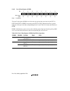
Table 19.8 Port D Data Register (PDDR) Read/Write Operations
PDnMD1 PDnMD0 Pin State Read Write
0 0 Other function
(see table 18.1)
PDDR value Value is written to PDDR, but does not
affect pin state
1 Output PDDR value Write value is output from pin
1 0 Input (Pull-up
MOS on)
Pin state Value is written to PDDR, but does not
affect pin state
1 Input (Pull-up
MOS off)
Pin state Value is written to PDDR, but does not
affect pin state
(n = 0, 1, 2, 3, 5, 7)
PDnMD1 PDnMD0 Pin State Read Write
0 0 Other function
(see table 18.1)
Low level Ignored (no effect on pin state)
1 Reserved Low level Ignored (no effect on pin state)
1 0 Input (Pull-up
MOS on)
Pin state Ignored (no effect on pin state)
1 Input (Pull-up
MOS off)
Pin state Ignored (no effect on pin state)
(n = 4, 6)


