Rev. 5.00, 09/03, page 204 of 760
9.2 Overview of CPG
9.2.1 CPG Block Diagram
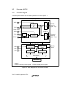
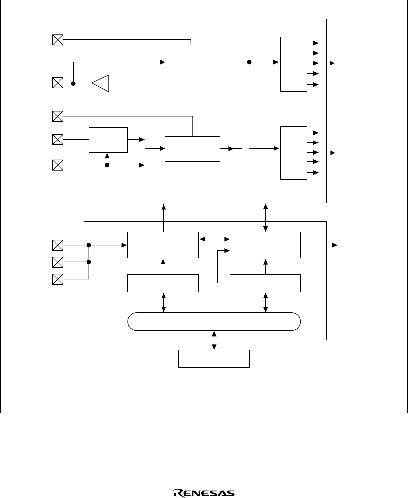
A block diagram of the on-chip clock pulse generator is shown in figure 9.1.
CAP1
CKIO
Cycle = Bcyc
CAP2
XTAL
EXTAL
MD2
MD1
MD0
FRQCR
Internal bus
Bus interface
STBCR
PLL circuit 1
(× 1, 2, 3, 4,
6)
Divider 1
Internal
clock (Iφ)
Cycle = Icyc
Peripheral
clock (Pφ)
Cycle = Pcy
c
Standby
control
Divider 2
Clock pulse generator
PLL circuit 2
(× 1, 4)
Crystal
oscillator
CPG control unit
Clock frequency
control circuit
Standby control
circuit
× 1
× 1/2
× 1/3
× 1/4
× 1/6
× 1
× 1/2
× 1/3
× 1/4
× 1/6
Legend
FRQCR: Frequency control register STBCR: Standby control register
Figure 9.1 Block Diagram of Clock Pulse Generator


