Rev. 5.00, 09/03, page 682 of 760
CKIO
A12 or A10
RD/WR
CSn
RAS
CAS
BS
DQMxx
CKE (High)
A25 to A16
A15 to A0
Tr Trw Trw
Tc1 Tcw Td1 (Tpc) (Tpc)
D31 to D0
Row address
Row address
Read A
command
Row address Column address
tAD
tAD
tAD tAD
tCSD3
tRWD
tDQMD
tRDH2
tBSDtBSD
tRDS2
tCSD3
tRWD
tRASD2
tDQMD
tRASD2
tCASD2 tCASD2
tAD
tAD
tAD
tAD
DACKn
t
DAKD1
t
DAKD1
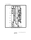
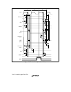
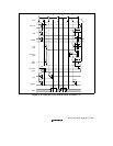
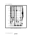
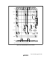
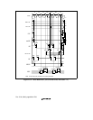
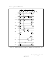
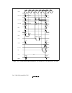
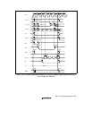
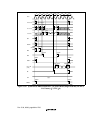
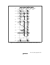
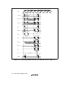
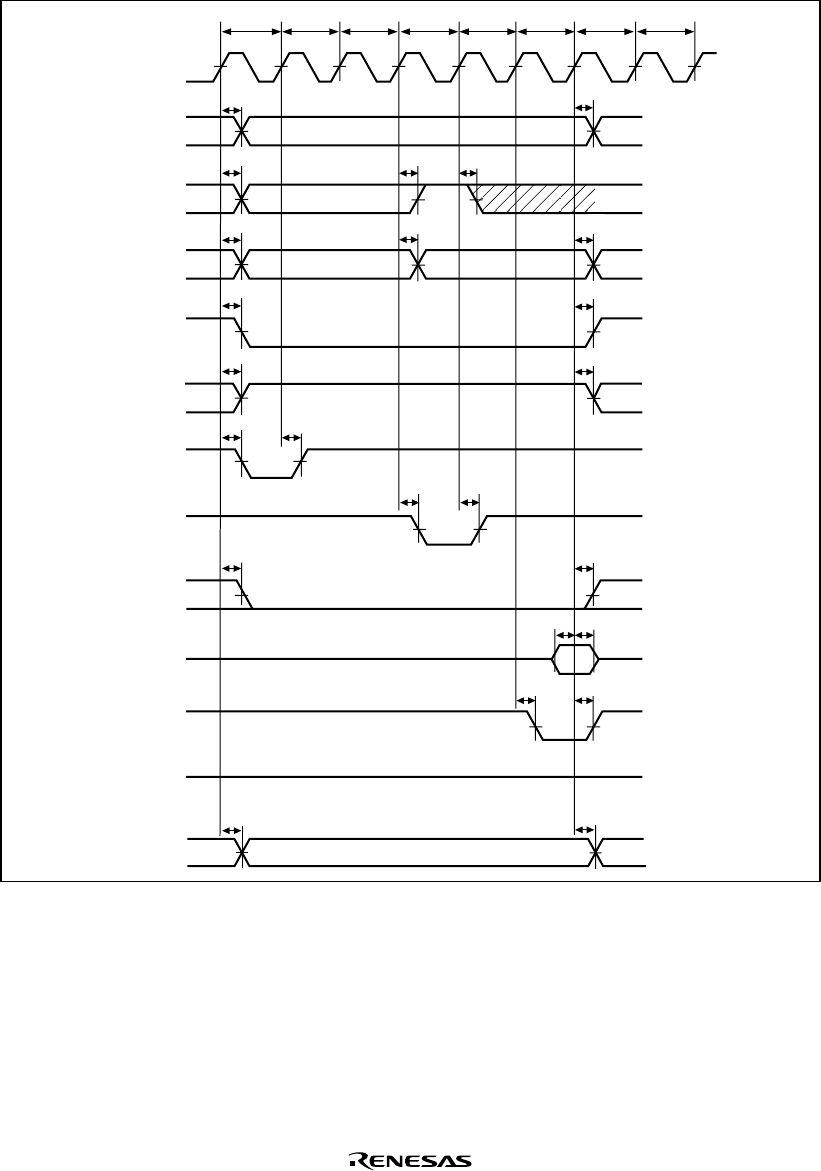
Figure 23.23 Synchronous DRAM Read Bus Cycle (RCD =
==
= 2, CAS Latency =
==
= 2, TPC =
==
= 1)


