Rev. 5.00, 09/03, page 621 of 760
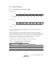
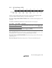
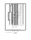
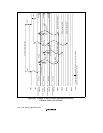
20.2.3 A/D Control Register (ADCR)
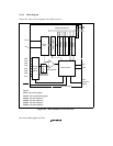
Bit:76543210
TRGE1 TRGE0 SCN RESVD1 RESVD2 — — —
Initial value:00000111
R/W: R/W R/W R/W R/W R/W R R R
ADCR is an 8-bit readable/writable register that enables or disables external triggering of A/D
conversion. ADCR is initialized to H'07 by a reset and in standby mode.
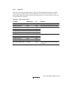
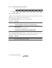
Bit 7 and 6—Trigger Enable (TRGE1, TRGE0): Enables or disables external triggering of A/D
conversion.
The TRGE1 and TRGE0 bits should only be set when conversion is not in progress.
Bit 7: TRGE1 Bit 6: TRGE0 Description
00
01
A/D conversion does not start when an external trigger is input
(Initial value)
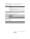
10
11
A/D conversion starts at the falling edge of an input signal from
the external trigger pin (ADTRG)
Bit 5—Scan Mode (SCN): Selects multi mode or scan mode when the MULTI bit is set to 1. See
the description of bit 4 in section 20.2.2, A/D Control/Status Register (ADCSR).
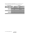
Bits 4 and 3—Reserved (RESVD1, RESVD2): These bits are always read as 0. The write value
should always be 0.
Bits 2 to 0—Reserved: These bits are always read as 1. The write value should always be 1.


