Rev. 5.00, 09/03, page 702 of 760
t
RDS1
t
RSD
CKIO
T
pcm0
T
pcm1
T
pcm1w
T
pcm1w
T
pcm1w
T
pcm2
T
pcm1
T
pcm1w
T
pcm2
T
pcm2w
A25 to A4
A3 to A0
CExx
RD/WR
RD
(read)
D15 to D0
(read)
Note: Even though burst mode is set, the write cycle operation is the same as in normal mode.
BS
DACKn
WAIT
t
AD
t
AD
t
CSD1
t
RWD
t
CSD1
t
DAKD1
t
RWD
t
AD
t
AD
t
AD
t
RSD
t
RSD
t
RSD
t
DAKD1
t
BSD
t
BSD
t
BSD
t
BSD
t
RDH1
t
RDH1
t
RDS1
t
WTS
t
WTH
t
WTS
t
WTS
t
WTH
t
WTH
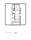
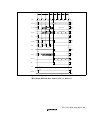
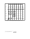
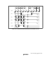
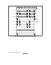
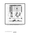
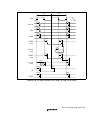
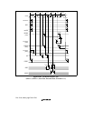
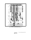
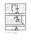
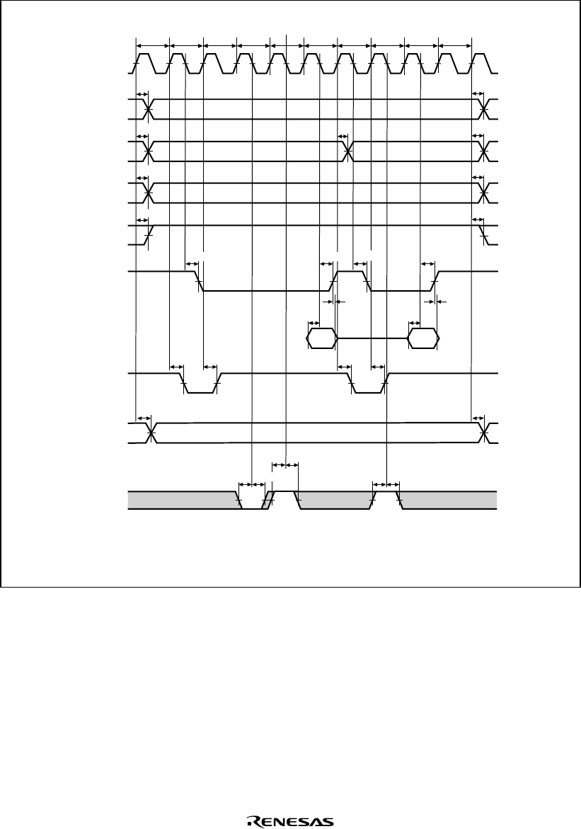
Figure 23.43 PCMCIA Memory Bus Cycle
(Burst Read, TED = 1, TEH = 1, Two Waits, Burst Pitch = 3, WAITSEL = 1)


