Rev. 5.00, 09/03, page 432 of 760
14.1.4 Register Configuration
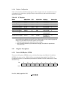
Table 14.2 summarizes the SCI internal registers. These registers select the communication mode
(asynchronous or synchronous), specify the data format and bit rate, and control the transmitter
and receiver sections.
Table 14.2 SCI Registers
Name Abbreviation R/W Initial Value Address Access size
Serial mode register SCSMR R/W H'00 H'FFFFFE80 8
Bit rate register SCBRR R/W H'FF H'FFFFFE82 8
Serial control register SCSCR R/W H'00 H'FFFFFE84 8
Transmit data register SCTDR R/W H'FF H'FFFFFE86 8
Serial status register SCSSR R/(W)
*
H'84 H'FFFFFE88 8
Receive data register SCRDR R H'00 H'FFFFFE8A 8
SC port data register SCPDR R/W H'00 H'04000136
(H'A4000136)
*
2
8
SC port control register SCPCR R/W H'A888 H'04000116
(H'A4000116)
*
2
16
Notes: These registers are located in area 1 of physical space. Therefore, when the cache is on,
either access these registers from the P2 area of logical space or else make an appropriate
setting using the MMU so that these registers are not cached.
1. The only value that can be written is 0 to clear the flags.
2. When address translation by the MMU does not apply, the address in parentheses
should be used.
14.2 Register Descriptions
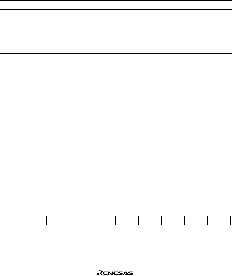
14.2.1 Receive Shift Register (SCRSR)
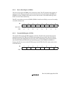
The receive shift register (SCRSR) receives serial data. Data input at the RxD pin is loaded into
SCRSR in the order received, LSB (bit 0) first, converting the data to parallel form. When one
byte has been received, it is automatically transferred to SCRDR. The CPU cannot read or write to
SCRSR directly.
Bit:76543210
R/W:————————


