Rev. 5.00, 09/03, page 495 of 760
15.3.2 Pin Connections
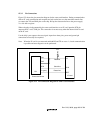
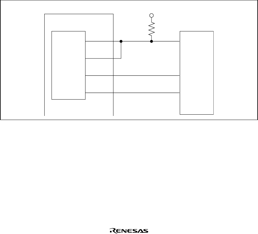
Figure 15.2 shows the pin connection diagram for the smart card interface. During communication
with an IC card, transmission and reception are both carried out over the same data transfer line,
so connect the TxD and RxD pins on the chip. Pull up the data transfer line to the power supply
V
CC
side with a register.
When using the clock generated by the smart card interface on an IC card, input the SCK pin
output to the IC card’s CLK pin. This connection is not necessary when the internal clock is used
on the IC card.
Use the chip’s port output as the reset signal. Apart from these pins, power and ground pin
connections are usually also required.
Note: When the IC card is not connected and both RE and TE are set to 1, closed communication
is possible and auto-diagnosis can be performed.
LSI
TxD
IO
CLK
RST
RxD
SCK
Px (port)
Clock line
Data line
Reset line
IC card
Connected device
V
CC
Figure 15.2 Pin Connection Diagram for Smart Card Interface


