Rev. 5.00, 09/03, page 520 of 760
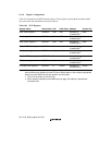
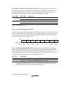
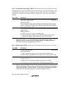
Bits 1 and 0—Clock Select 1 and 0 (CKS1, CKS0): Select the internal clock source of the on-
chip baud rate generator. According to the setting of the CKS1 and CKS0 bits four clock sources
are available. Pφ, Pφ/4, Pφ/16 and Pφ/64. For further information on the clock source, bit rate
register settings, and baud rate, see section 16.2.8, Bit Rate Register (SCBRR).
Bit 1: CKS1 Bit 0: CKS0 Description
00Pφ (Initial value)
1Pφ/4
10Pφ/16
1Pφ/64
Note: Pφ: Peripheral clock
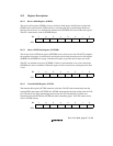
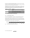
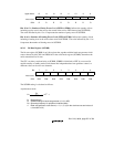
16.2.6 Serial Control Register (SCSCR)
The serial control register (SCSCR) operates the SCIF transmitter/receiver, selects the serial clock
output in asynchronous mode, enables/disables interrupt requests, and selects the transmit/receive
clock source. The CPU can always read and write to SCSCR. SCSCR is initialized to H'00 by a
reset and in standby or module standby mode.
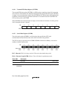
Bit:76543210
TIE RIE TE RE — — CKE1 CKE0
Initial value:00000000
R/W: R/W R/W R/W R/W R R R/W R/W
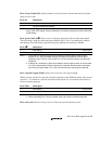
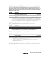
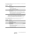
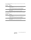
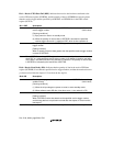
Bit 7—Transmit Interrupt Enable (TIE): Enables or disables the transmit-FIFO-data-empty
interrupt (TXI) requested when the serial transmit data is transferred from the transmit FIFO data
register (SCFTDR) to the transmit shift register (SCTSR), when the quantity of data in the
transmit FIFO register becomes less than the specified number of transmission triggers, and when
the TDFE flag in the serial FIFO status register (SCFSR) is set to1.
Bit 7: TIE Description
0 Transmit-FIFO-data-empty interrupt request (TXI) is disabled
*
(Initial value)
1 Transmit-FIFO-data-empty interrupt request (TXI) is enabled
Note: * The TXI interrupt request can be cleared by writing a greater quantity of transmit data than
the specified transmission trigger number to SCFTDR and by clearing TDFE to 0 after
reading 1 from TDFE, or can be cleared by clearing TIE to 0.


