Rev. 5.00, 09/03, page 513 of 760
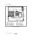
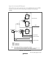
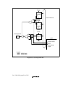
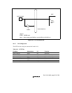
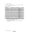
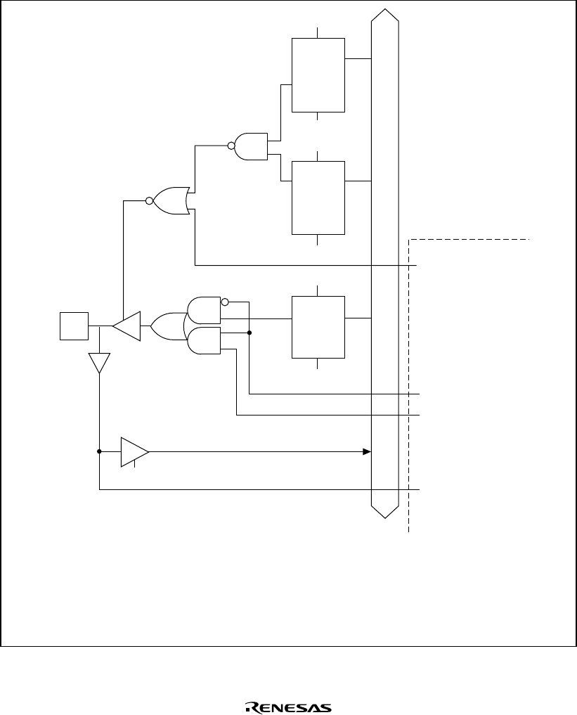
Figures 16.2 to 16.4 show the SCIF I/O port pins.
SCIF pin I/O and data control is performed by bits 11 to 8 of SCPCR and bits 5 and 4 of SCPDR.
For details, see section 14.2.8, SC Port Control Register (SCPCR)/SC Port Data Register
(SCPDR).
Internal data bus
Output enable
Clock input enable
SCIF
Serial clock output
Serial clock input
R
SCP5MD0
PCRW
Reset
C
Q
Q
D
R
SCP5MD1
PCRW
Reset
C
Q D
R
SCP5DT1
PDRW
Reset
SCPT[5]/SCK2
C
D
PDRW:
Legend
SCPDR write
PDRR:
PCRW:
SCPDR read
SCPCR write
PDRR*
Note: * When reading the SCK2 pin, clear the CKE1 and CKE0
bits in SCSCR to 0, and set the SCP5MD1 bit in SCSPR to 1 (see section 14.2.8,
SC Port Control Register (SCPCR)/SC Port Data Register (SCPDR)).
Figure 16.2 SCPT[5]/SCK2 Pin


