Rev. 5.00, 09/03, page 3 of 760
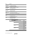
Item Features
Cache memory
• 16-kbyte cache, mixed instruction/data
• 256 entries, 4-way set associative, 16-byte block length
• Write-back, write-through, LRU replacement algorithm
• 1-stage write-back buffer
• Maximum 2 ways of the cache can be locked
Interrupt
controller (INTC)
• 23 external interrupt pins (NMI, IRQ5–IRQ0, PINT15 to PINT0)
• On-chip peripheral interrupts: set priority levels for each module
User break
controller (UBC)
• 2 break channels
• Addresses, data values, type of access, and data size can all be set as break
conditions
• Supports a sequential break function
Bus state
controller (BSC)
• Physical address space divided into six areas (area 0, areas 2 to 6), each a
maximum of 64 Mbytes, with the following features settable for each area:
Bus size (8, 16, or 32 bits)
Number of wait cycles (also supports a hardware wait function)
Setting the type of space enables direct connection to SRAM,
Synchronous DRAM, and burst ROM
Supports PCMCIA interface (2 channels)
Outputs chip select signal (CS0, CS2–CS6) for corresponding area
• Synchronous DRAM refresh function
Programmable refresh interval
Support self-refresh mode
• Synchronous DRAM burst access function
• Usable as either big or little endian machine
User-debugging
Interface (UDI)
• E10A emulator support
• JTAG-compliant
• Realtime branch address trace
• 1-kB on-chip RAM for fast emulation program execution
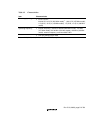
Timer (TMU)
• 3-channel auto-reload-type 32-bit timer
• Input capture function
• 6 types of counter input clocks can be selected
• Maximum resolution: 2 MHz
Realtime clock
(RTC)
• Built-in clock, calendar functions, and alarm functions
• On-chip 32-kHz crystal oscillator circuit with a maximum resolution (interrupt
cycle) of 1/256 second


