Rev. 5.00, 09/03, page 657 of 760
Section 23 Electrical Characteristics
23.1 Absolute Maximum Ratings
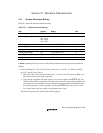
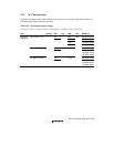
Table 23.1 shows the absolute maximum ratings.
Table 23.1 Absolute Maximum Ratings
Item Symbol Rating Unit
Power supply voltage (I/O) VccQ –0.3 to 4.2 V
Power supply voltage (internal) Vcc
Vcc – PLL1
Vcc – PLL2
Vcc – RTC
–0.3 to 2.5 V
Input voltage (except port L) Vin –0.3 to VccQ + 0.3 V
Input voltage (port L) Vin –0.3 to AVcc + 0.3 V
Analog power-supply voltage AVcc –0.3 to 4.6 V
Analog input voltage V
AN
–0.3 to AVcc + 0.3 V
Operating temperature Topr –20 to 75 °C
Storage temperature Tstr –55 to 125 °C
Caution: Operating the chip in excess of the absolute maximum rating may result in permanent
damage.
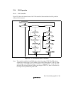
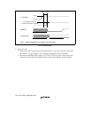
• Order of turning on 1.7 V/1.8 V/1.9 V/2.0 V power (Vcc, Vcc-PLL1, Vcc-PLL2, Vcc-RTC)
and 3.3 V power (VccQ, AVcc):
1. First turn on the 3.3 V power, then turn on the 1.7 V/1.8 V/1.9 V/2.0 V power within 1 ms.
This interval should be as short as possible.
2. Until voltage is applied to all power supplies, a low level is input at the RESETP pin, and
CKIO has operated for a maximum of 4 clock cycles, internal circuits remain unsettled, and
so pin states are also undefined. The system design must ensure that these undefined states
do not cause erroneous system operation. Note that the RESETP pin cannot receive a low
level signal while a low level signal is being input to the CA pin.
Waveforms at power-on are shown in the following figure.


