Rev. 5.00, 09/03, page 304 of 760
10.3.5 Burst ROM Interface
Setting bits A0BST1–0, A5BST1–0, and A6BST1–0 in BCR1 to a non-zero value allows burst
ROM to be connected to areas 0, 5, and 6. The burst ROM interface provides high-speed access to
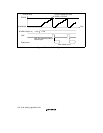
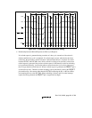
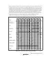
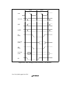
ROM that has a nibble access function. The timing for nibble access to burst ROM is shown in
figure 10.29. Two wait cycles are set. Basically, access is performed in the same way as for
normal space, but when the first cycle ends the CS0 signal is not negated, and only the address is
changed before the next access is executed. When 8-bit ROM is connected, the number of
consecutive accesses can be set as 4, 8, or 16 by bits A0BST1–0, A5BST1–0, or A6BST1–0.
When 16-bit ROM is connected, 4 or 8 can be set in the same way. When 32-bit ROM is
connected, only 4 can be set.
WAIT pin sampling is performed in the first access if one or more wait states are set, and is
always performed in the second and subsequent accesses.
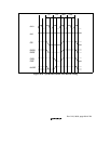
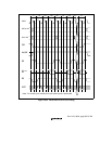
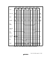
The second and subsequent access cycles also comprise two cycles when a burst ROM setting is
made and the wait specification is 0. The timing in this case is shown in figure 10.30.
However, the WAIT signal is ignored in the following three cases:
• A write to external address space in dual address mode with 16-byte DMA transfer
• Transfer from an external device with DACK to external address space in single address mode
with 16-byte DMA transfer
• Cache write-back access


