Rev. 5.00, 09/03, page 444 of 760
14.2.8 SC Port Control Register (SCPCR)/SC Port Data Register (SCPDR)
The SC port control register (SCPCR) and SC port data register (SCPDR) control I/O and data for
the port pins multiplexed with the serial communication interface (SCI) pins.
SCPCR settings are used to perform I/O control, to enable data written in SCPDR to be output to
the TxD pin, and input data to be read from the RxD pin, and to control serial
transmission/reception breaks.
It is also possible to read data on the SCK pin, and write output data.
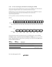
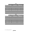
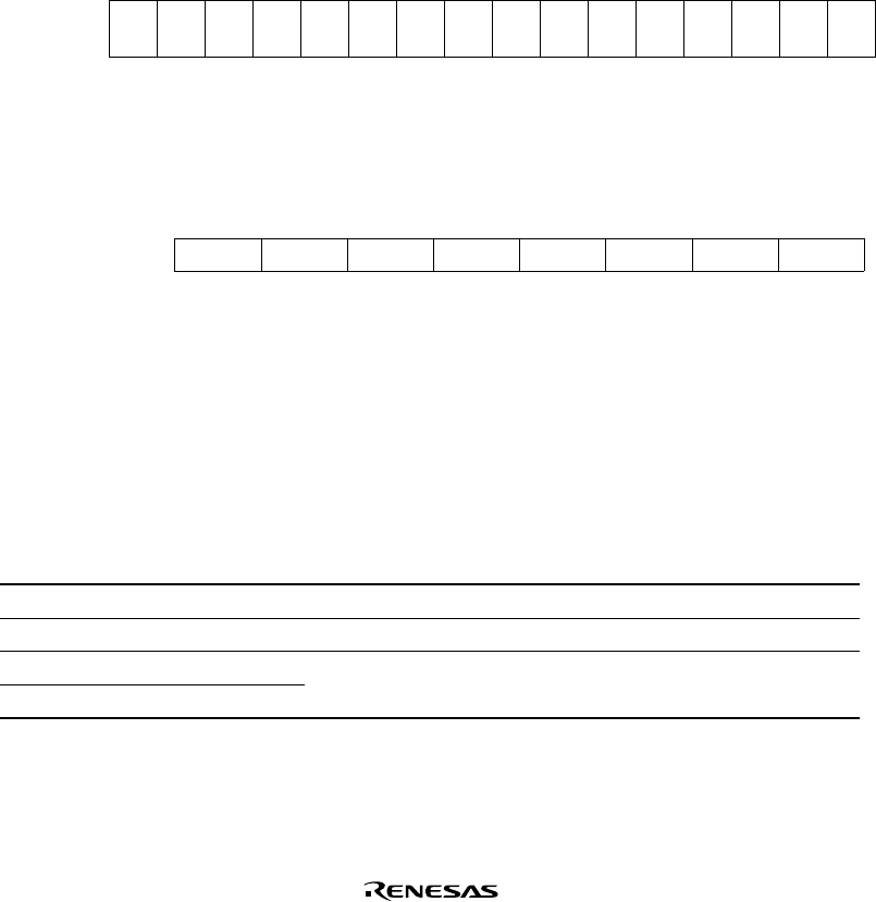
SCPCR
Bit:1514131211109876543210
SCP7
MD1
SCP7
MD0
SCP6
MD1
SCP6
MD0
SCP5
MD1
SCP5
MD0
SCP4
MD1
SCP4
MD0
SCP3
MD1
SCP3
MD0
SCP2
MD1
SCP2
MD0
SCP1
MD1
SCP1
MD0
SCP0
MD1
SCP0
MD0
Initial value:1010100010001000
R/W: R/W R/W R/W R/W R/W R/W R/W R/W R/W R/W R/W R/W R/W R/W R/W R/W
SCPDR
Bit:76543210
SCP7DT SCP6DT SCP5DT SCP4DT SCP3DT SCP2DT SCP1DT SCP0DT
Initial value:00000000
R/W: R R/W R/W R/W R/W R/W R/W R/W
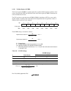
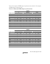
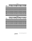
SCI pin I/O and data control are performed by bits 3–0 of SCPCR and bits 1 and 0 of SCPDR.
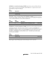
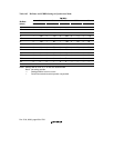
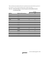
SCPCR Bits 3 and 2—Serial Clock Port I/O (SCP1MD1, SCP1MD0): Specify serial port SCK
pin I/O. When the SCK pin is actually used as a port I/O pin, clear the C/A bit in SCSMR and bits
CKE1 and CKE0 in SCSCR to 0.
Bit 3:
SCP1MD1
Bit 2:
SCP1MD0 Description
0 0 SCP1DT bit value is not output to SCK pin
0 1 SCP1DT bit value is output to SCK pin
1 0 SCK pin value is read from SCP1DT bit
1 1 (Initial values: 1 and 0)


