Rev. 5.00, 09/03, page 516 of 760
16.1.4 Register Configuration
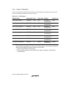
Table 16.2 summarizes the SCIF internal registers. These registers specify the data format and bit
rate, and control the transmitter and receiver sections.
Table 16.2 SCIF Registers
Register Name Abbreviation R/W Initial Value Address Access size
Serial mode register 2 SCSMR2 R/W H'00 H'04000150
(H'A4000150)
*
2
8 bits
Bit rate register 2 SCBRR2 R/W H'FF H'04000152
(H'A4000152)
*
2
8 bits
Serial control register 2 SCSCR2 R/W H'00 H'04000154
(H'A4000154)
*
2
8 bits
Transmit FIFO data register 2 SCFTDR2 W — H'04000156
(H'A4000156)
*
2
8 bits
Serial status register 2 SCSSR2 R/(W)
*
1
H'0060 H'04000158
(H'A4000158)
*
2
16 bits
Receive FIFO data register 2 SCFRDR2 R Undefined H'0400015A
(H'A400015A)
*
2
8 bits
FIFO control register 2 SCFCR2 R/W H'00 H'0400015C
(H'A400015C)
*
2
8 bits
FIFO data count register 2 SCFDR2 R H'0000 H'0400015E
(H'A400015E)
*
2
16 bits
Notes: These registers are located in area 1 of physical space. Therefore, when the cache is on,
either access these registers from the P2 area of logical space or else make an appropriate
setting using the MMU so that these registers are not cached.
1. Only 0 can be written to clear the flag.
2. When address translation by the MMU does not apply, the address in parentheses
should be used.


