Rev. 5.00, 09/03, page 643 of 760
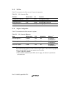
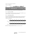
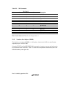
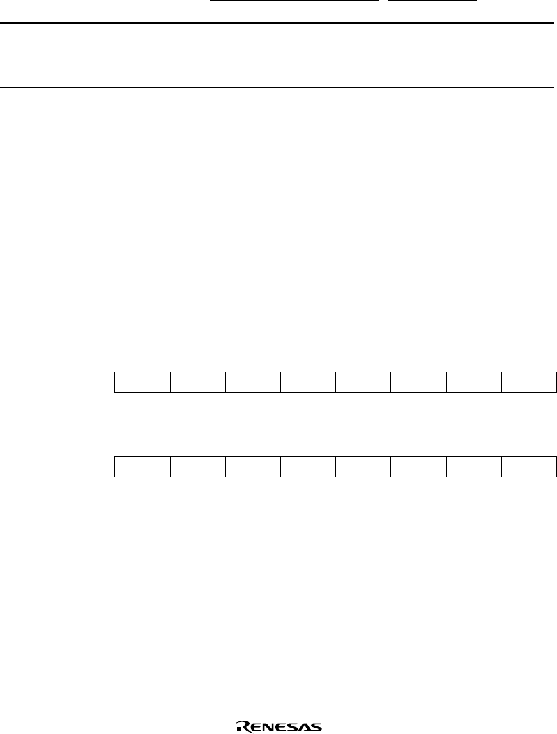
Table 22.1 shows the UDI register configuration.
Table 22.1 UDI Registers
CPU Side UDI Side
Initial
Name Abbreviation R/W Size Address R/W Size Value
*
Bypass register SDBPR — — — R/W 1 Undefined
Instruction register SDIR R 16 H'04000200 R/W 16 H'FFFF
Boundary register SDBSR — — — R/W — Undefined
Note: * Initialized when TRST pin is low or when TAP is in the test-logic-reset state.
22.3.1 Bypass Register (SDBPR)
The bypass register is a 1-bit register that cannot be accessed by the CPU. When SDIR is set to the
bypass mode, SDBPR is connected between UDI pins TDI and TDO.
22.3.2 Instruction Register (SDIR)
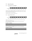
The instruction register (SDIR) is a 16-bit read-only register. The register is in bypass mode in its
initial state. It is initialized by TRST assertion or in the TAP test-logic-reset state, and can be
written to by the UDI irrespective of the CPU mode. Operation is not guaranteed if a reserved
command is set in this register
Bit: 15 14 13 12 11 10 9 8
TI3TI2TI1TI0————
Initial value:11111111
Bit:76543210
————————
Initial value:11111111
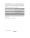
Bits 15 to 12—Test Instruction Bits (TI3 to TI0): Cannot be written by the CPU.


