Rev. 5.00, 09/03, page 681 of 760
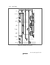
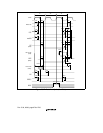
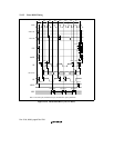
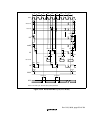
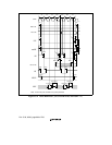
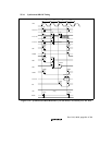
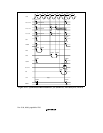
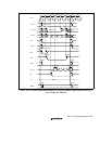
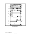
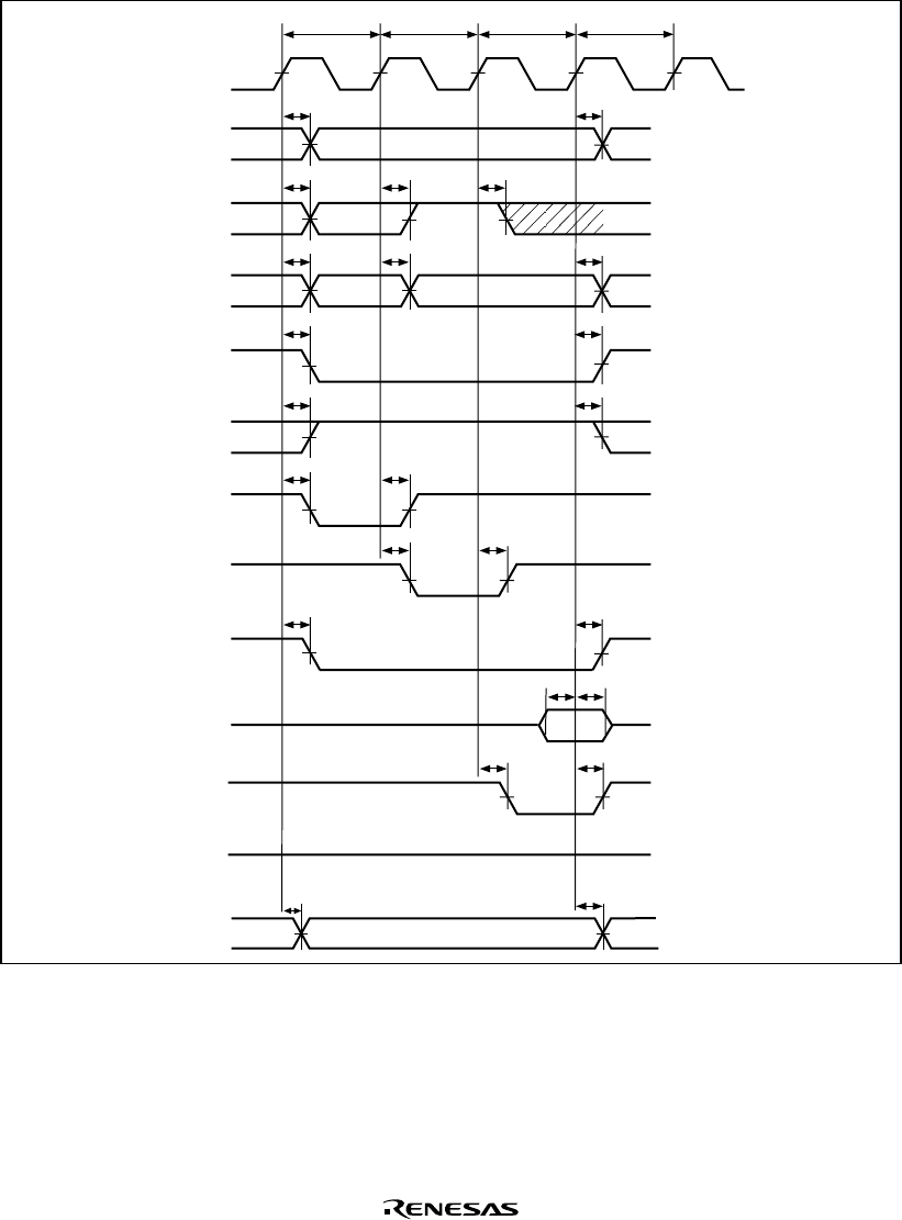
23.3.6 Synchronous DRAM Timing
CKIO
A12 or A10
RD/WR
CSn
RAS
CAS
BS
DQMxx
CKE
A25 to A16
A15 to A0
Tr
tAD
Row address
Row address
Read A
command
Row address Column address
Tc1 Tc2
(Tpc)
D31 to D0
tAD
tAD tAD
tAD
tCSD3
tRWD
tCSD3
tRWD
tRASD2
tDQMD tDQMD
tRDH2
tBSDtBSD
(High)
tRDS2
tRASD2
tCASD2 tCASD2
tAD tAD
tAD
D
ACKn
t
DAKD1
t
DAKD1
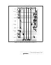
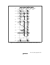
Figure 23.22 Synchronous DRAM Read Bus Cycle (RCD =
==
= 0, CAS Latency =
==
= 1, TPC =
==
= 0)


