Rev. 5.00, 09/03, page 632 of 760
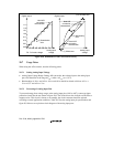
111
110
101
100
011
010
001
000
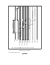
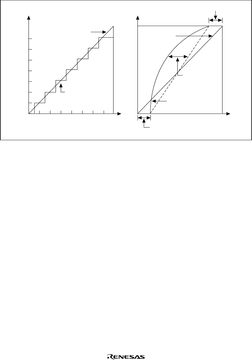
0 1/8 2/8 3/8 4/8 5/8 6/8 7/8 FS
Analog input
voltage
FS: Full-scale voltage
(3) Quantization
error
Ideal A/D
conversion
characteristic
(4) Nonlinearity
error
Ideal A/D
conversion
characteristic
Actual A/D
convertion
characteristic
(2) Full-scale erro
r
Digital output
Analog input
voltage
(1) Offset error
FS
Digital output
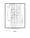
Figure 20.8 Definitions of A/D Conversion Accuracy
20.7 Usage Notes
When using the A/D converter, note the following points.
20.7.1 Setting Analog Input Voltage
• Analog Input Voltage Range: During A/D conversion, the voltages input to the analog input
pins ANn should be in the range AV
SS
≤ ANn ≤ AV
CC
(n = 0 to 7).
• Relationships of AV
CC
and AV
SS
: AV
CC
and AV
SS
should be related as follows: AV
CC
=
V
CC
± 0.3 V and AV
SS
= V
SS
.
20.7.2 Processing of Analog Input Pins
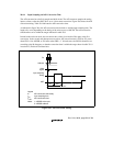
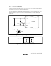
To prevent damage from voltage surges at the analog input pins (AN0 to AN7), connect an input
protection circuit like the one shown in figure 20.9. The circuit shown also includes an CR filter to
suppress noise. This circuit is shown as an example; the circuit constants should be selected
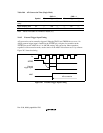
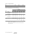
according to actual application conditions. Table 20.5 lists the analog input pin specifications and
figure 20.10 shows an equivalent circuit diagram of the analog input ports.


