Rev. 5.00, 09/03, page 629 of 760
20.4.4 Input Sampling and A/D Conversion Time
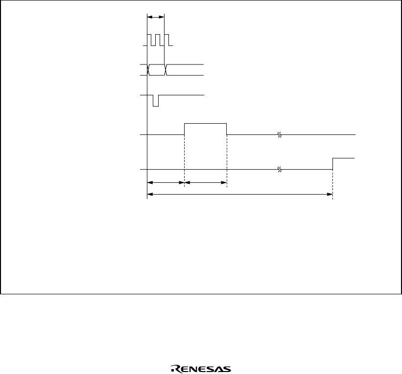
The A/D converter has a built-in sample-and-hold circuit. The A/D converter samples the analog
input at a time t
D
after the ADST bit is set to 1, then starts conversion. Figure 20.6 shows the A/D
conversion timing. Table 20.4 indicates the A/D conversion time.
As indicated in figure 20.6, the A/D conversion time includes t
D
and the input sampling time. The
length of t
D
varies depending on the timing of the write access to ADCSR. The total conversion
time therefore varies within the ranges indicated in table 20.4.
In multi mode and scan mode, the conversion time values given in table 20.4 apply to the first
conversion. In the second and subsequent conversions, the conversion time is fixed at 512 states
when CKS = 0 in ADCSR, or 256 states when CKS = 1. In both cases, the CKS bit should be set
according to the Pφ frequency so that the conversion time is within the range shown in table 23.10
in section 23, Electrical Characteristics.
P
φ
Write
signal
ADF
*1
Input sampling
timing
Legend
t
D
A/D conversion start delay
t
SPL
Input sampling time
t
CONV
A/D conversion time
Notes: 1. ADCSR write cycle
2. ADCSR address
Address
*2
t
D
t
SPL
t
CONV
Figure 20.6 A/D Conversion Timing
