Rev. 5.00, 09/03, page 290 of 760
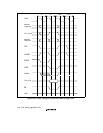
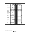
A Tnop cycle, in which no operation is performed, is inserted before the Tc cycle in which the
READ command is issued in figure 10.20, but when synchronous DRAM is read, there is a two-
cycle latency for the DQMxx signal that performs the byte specification. If the Tc cycle were
performed immediately, without inserting a Tnop cycle, it would not be possible to perform the
DQMxx signal specification for Td1 cycle data output. This is the reason for inserting the Tnop
cycle. If the CAS latency is two cycles or longer, Tnop cycle insertion is not performed, since the
timing requirements will be met even if the DQMxx signal is set after the Tc cycle.
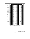
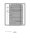
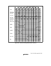
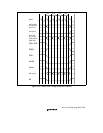
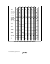
When bank active mode is set, if only accesses to the respective banks in the area 3 space are
considered, as long as accesses to the same row address continue, the operation starts with the
cycle in figure 10.19 or 10.22, followed by repetition of the cycle in figure 10.20 or 10.23. An
access to a different area 3 space during this time has no effect. If there is an access to a different
row address in the bank active state, after this is detected the bus cycle in figure 10.21 or 10.24 is
executed instead of that in figure 10.20 or 10.23. In bank active mode, too, all banks become
inactive after a refresh cycle or after the bus is released as the result of bus arbitration.
The bank active mode should not be used unless the bus width for all areas is 32 bits.


