


Theory of Operation
3–72
AM700 Audio Measurement Set Service Manual
By design, the voltage level required to shut off the PWM is low compared to
the high logic level from the Shutdown gate. A diode clamping circuit formed by
R24 and CR14 prevents the SD level from exceeding the forward bias drop of
the diode, about 0.6 V. Capacitor C25 bypasses fast transients from the SD input.
The pulse-width modulated outputs of PWM U1 are at pins 11 and 14. The
output pulses are buffered by the high-current FET driver device, U6, whose
output pins 12 and 13 drive the primary of T2. The secondaries of transformer
T2 drive the gates of the pulse-width modulated switching FET, Q2 and Q3.
The leading edges of the pulses from U1, pins 11 and 14, are also used to trigger
comparator U4A. The comparator output clocks U5A, a D-type flip-flop
configured as a toggling circuit that changes state with clock. This circuit is used
to derive the 50% duty cycle pulses which are also buffered by U6. These
outputs drive the primary of T3 which, in turn, drives the gates of inverter
switching FET Q6 and Q7.
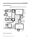
The preregulator consists of T2, Q2, Q3, L4, CR23, C31, and C32. Parallel FET
transistors, Q2 and Q3 are driven alternately, each at a 50 kHz rate. The gates of
Q2 and Q3 are driven by the Pulse-Width Modulator (PWM), U1, through FET
driver U6 and pulse transformer T2.
Transformer T4 and transistors Q4 and Q5 form a current sense circuit that
functions to sense the current in the step-down inductor L4. This circuit provides
a scaled-down replica of the switching FET current to pin 4 of PWM U1.
The inverter consists of T5, Q6, and Q7. FET transistors Q6 and Q7 are also
driven alternately, each at 50 kHz, and provide a 50 kHz switching rate to the
primary of T5. They are not pulse-width modulated, but driven at a 50% duty
cycle, through pulse transformer T3. Drive to the pulse transformers, T2 and T3,
is supplied by U6, a high-current FET driver device. The inverter is driven in a
one-half bridge configuration. Capacitors C31 and C32 divide the full voltage at
L4 by 1/2, and the voltage across each capacitor is alternately applied to the
primary winding of transformer T5 through the switching action of Q6 and Q7.
This configuration produces a self-correcting circuit action that equalizes the
positive and negative voltage swings seen by the primary of T5 and keeps it out
of saturation.
The approximately 180 V, square-wave voltage across the primary winding of
switching transformer T5 is stepped down in two center-tapped secondaries to
provide drive to the +5 V, ±16.5 V, and ±22 V rectifier and filter circuits. The
16.5 V secondary voltage supplies the +15 V Series-Pass Regulator.
Power Switch Driver
Preregulator
Current Sensing
Inverter
Output Rectifiers and
Filtering