


Theory of Operation
AM700 Audio Measurement Set Service Manual
3–57
The DSP clock generator has 33.333 MHz applied as the reference frequency.
The clock generator develops the various clock signals used throughout the DSP
board.
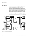
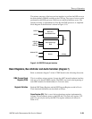
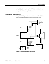
Bus Buffers and Connectors (diagram 1)
The bus buffers handle the 32 bit data and address busses between the DSP and
the main CPU.
Reset and Clocks (diagram 2)
Refer to schematic diagram 2 of the A7 DSP board for the following discussion.
The System Reset logic circuitry has inputs of CPU RST, RSTON, RST, and
input from the Master Reset switch S1, to develop the DSPRST signal to the
DSP. A power-on monitor, U17, holds the RST signal low until the +5 V has
stabilized. This hold the DSP in the reset condition until all the circuitry is ready
to operate correctly. The Master Reset switch, S1, may be pressed to cause the
DSP circuitry to be reset. Pressing the reset button, resets the DSP and its
peripherals. The host CPU and its related circuitry are not affected by this reset.
There are five input sources that can assert the RESET pin of DSP and reset its
interface circuitry. They are as follows:
H ONCE Interface reset (not used),
H Board Program Register BPR (bit 5),
H Power-Up Reset Controller,
H DSP Reset button,
H Port B host port reset.
The DSP is placed in the reset state upon initial application of power and will
remain in this state until the CPU deasserts the reset pin of the DSP by writing a
‘1’ to bit 5 of the Board Program Register. Upon leaving the reset state, the
processor bootstraps through Port B, the Host Interface.
The DSP clock generator, U19, has 33.333 MHz from a divide-by-two circuit
applied as the reference frequency. The clock generator develops the various
clock signals used throughout the DSP board.
System Reset
DSP Reset Functional
Description
Clock Generator