


Theory of Operation
3–36
AM700 Audio Measurement Set Service Manual
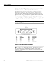
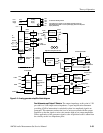
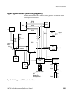
The generator DSP, U4, develops the digital data that represents the audio test
signal to output from the front panel Analog Generator XLR connectors. It is
programmed by the host CPU via the host interface. The data is clocked out
serially to the generator DACs through the SSI (synchronous serial interface) of
the DSP.
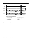
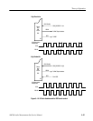
The Reset and SSI Clock Pal, U7, allows the output data to be clocked either
directly from the DSP or from a divided version of the 12.288 MHz clock
frequency. These two types of operation are the High Resolution mode and the
High Bandwidth mode. The SCK DISABLE signal controls switching between
the states as shown in Figure 3–13. The resulting waveforms of the clocks and
data stream for the two modes is shown in Figure 3–14. The High Resolution
mode sample rate is 48 kbits per second, and the High Bandwidth mode sample
rate is 192 kbits per second.
There are two chip enables and some memory addressing bits decoded by U5,
the Address Decoder. The chip enable signals are used to enable the Serial
Control Pal and the RAM, U2. The addressing bits (RA15, RA16, and RA17)
are applied to the RAM to control the upper three bits of the RAM addresses.
The RAM, U2, holds the programming for the test signals. The data is loaded
from the CPU through the DSP. Read and write control is provided from the
DSP RD and WR outputs. The chip enable signal (CERAM) is developed from
the Address Decoder, U5.
DSP
Reset and SSI Clock Pal
Address Decoder
RAM