


Theory of Operation
3–58
AM700 Audio Measurement Set Service Manual
Sample Receivers (diagram 3)
Refer to schematic diagram 3 of the A7 DSP board for the following discussion.
There are two sample receivers, U10 and U11. One handles the analog samples
and the other handles the digital signal. These sample receivers are identical to
the sample transmitters. A single control bit, TX/RX, defines the operating mode
of the ASICs. In the sample receivers, this bit is wired low. The sample receivers
accept 8-bit data from the acquisition system and formats it into 32-bit long
words for application to the DSP. Each sample receiver handles two channels of
input data. Output data is written to the shared RAM on Port A of the DSP. The
DSP handles the signal processing and transfer of the processed data to the CPU
for display in the running application.
A Memory (diagram 4)
Refer to schematic diagram 4 of the A7 DSP board for the following discussion.
The local memory residing on the Port A bus is organized in one bank of 128K ×
32 of fast static memory. It can be expanded to 256K × 32. This memory is
shared between the DSP and the sample receivers for transfer of the incoming
data to the DSP for processing. The processed data is then transferred to the CPU
through the host interface for display in the running application. Reads and
writes to this memory is controlled by the bus arbitration control PAL, U55
(shown on diagram 7).
B Memory (diagram 5)
Refer to schematic diagram 5 of the A7 DSP board for the following discussion.
The local memory residing on the Port B bus is organized in one bank of 128K ×
32 of fast static memory. It can be expanded to 256K × 32. Reads and writes to
the B Port RAM are controlled by the B Port Memory Controller, U32. This
memory is shared between the DSP and the CPU and is used for data transfers
between the two through the DSP/CPU interface ASIC, U15 (shown on
diagram 6).
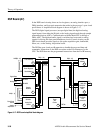
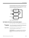
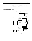
DSP/CPU Interface ASIC (diagram 6)
Refer to schematic diagram 6 of the A7 DSP board for the following discussion.
The ASIC consists of the three functional blocks shown in Figure 3–18. They are
the following: DMA interface, DSP Host Port interface, and local memory
controller. There is a built-in 32-bit Address Holding Register (AHR) in the
ASIC to set up various base addresses of the controlled functional blocks. The
default value (after power up/during reset is active) is $010560CC. The AHR is a
write-once/read-many register. It allows one write after reset.